Mixed voltage input/output buffer having low-voltage design

a low-voltage design and input/output buffer technology, applied in the direction of pulse technique, logic circuit, electrical pulse generator details, etc., can solve the problems of device size, power consumption of lower supply voltage, power supply voltage reduction of chip, etc., and achieve the effect of eliminating the reliability problem of gate oxide layer

Active Publication Date: 2009-05-12
NAT CHIAO TUNG UNIV
View PDF7 Cites 10 Cited by
  • Summary
  • Abstract
  • Description
  • Claims
  • Application Information

AI Technical Summary

Benefits of technology

[0009]The object of the present invention is to provide a mixed-voltage input / output buffer, which could be applied in a nano processor, and be composed of low voltage devices, and could prevent the undesired current leakage, the sub-threshold current leakage, and eliminate the reliability problem of gate oxide layer.
[0010]The present invention provides a mixed-voltage input / output buffer, which comprises a pre-driver, a tracking unit, a driving unit, and an input / output pad, a floating-well unit, and a transporting unit; wherein, the pre-driver receives a first data signal and an enable signal from an external unit, and outputs first and second data voltages; the tracking unit includes a switch device and a plurality of transistors providing the gate-tracking function, and these transistors are used to prevent the occurrence of current leakage in the switch device and the driving unit; the driving unit is used to generate a first buffer voltage corresponding to the first data voltage; the input / output pad is coupled with the driving unit to output a first buffer voltage to another external unit, and to receive a second data signal from an external unit, and the driving unit has a well as the substrate of the transistors in the driving unit; the transporting unit is used to output a second buffer voltage corresponding to the second data signal; and, the floating-well unit is coupled to the driving unit and the input / output pad for preventing current leakage in the well of the driving unit.
[0011]The present invention employs the composite structure by the tracking unit, the floating-well unit and the driving unit to eliminate the current leakage, so it could prevent the reliability problem of the gate oxide layer, avoid the undesired current leakage and the sub-threshold current leakage, and it employs the low voltage devices and is suitable for nano process.

Problems solved by technology

In the nano scale, the power supply voltage of chip is reduced; obviously, the reduction of device size not only makes the chip area smaller to save the silicon cost, but also the lower supply voltage will consume lower power.
In order for the compatibility of chips with different voltage levels, the input / output buffer in prior art was not suitable, and caused some problems, such as the reliability problem for gate oxide layer, deterioration of thermal carriers, and generation of undesired current leakage path.
The input / output buffer was subjected to current leakage, and the reliability problem of gate oxide layer.
However, it will increase the manufacturing cost for the chip having both the thick oxide layer devices and the thin oxide layer devices.
However, the DC current path in the transistors 107, 109 and 110 existed from voltage VDD to voltage VSS will cause additional power consumption, and using the stacked transistors 101, 102 will reduce the driving capability.
Moreover, the P-type MOS transistor 401 is a thick oxide layer (high voltage) device for preventing the reliability problem of the gate oxide layer, which will result in more cost and larger silicon area.
When the buffer driving voltage VDD is the output voltage, the voltage of the body for the P-type MOS transistor is the bias current value VDD minus from the threshold voltage Vt, it will result in large amount of sub-threshold current leakage.
Moreover, when the input / output buffer is receiving a high input voltage, the base voltage of the P-type MOS transistor will be biased through the parasitic diode 322, and further result in the occurrence of large amount of sub-threshold current leakage.

Method used


Image

  • Mixed voltage input/output buffer having low-voltage design
  • Mixed voltage input/output buffer having low-voltage design
  • Mixed voltage input/output buffer having low-voltage design

Examples


Embodiment Construction

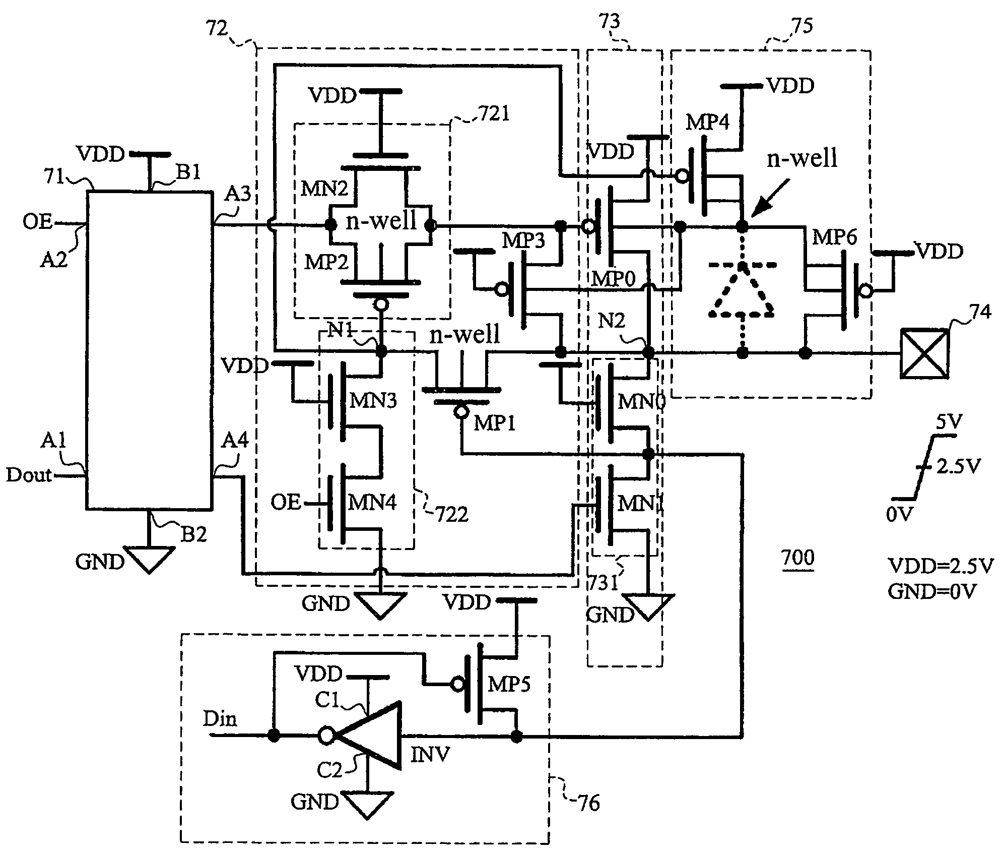
[0022]Now, please refer to FIG. 7 to describe the aspects of the present invention. FIG. 7 is a circuit diagram showing the mixed-voltage input / output buffer 700 having low-voltage design in an embodiment according to the present invention. The mixed-voltage input / output buffer 700 comprises a pre-driver 71, a tracking unit 72, a driving unit 73, input / output pad 74, a floating-well unit 75, and a transporting unit 76. The pre-driver 71 includes a data input terminal A1, a control terminal A2, a higher output port A3, and a lower output port A4, in which the data input terminal A1 of the pre-driver 71 receives a first data signal Dout from an external unit (not shown), and receives the enable signal OE through the control terminal A2. The pre-driver 71 will convert the first data signal Dout and the enable signal OE for outputting a first data voltage and a second data voltage from the higher output port A3 and the lower output port A4, respectively, wherein the first data voltage i...


PUM


Abstract

A mixed-voltage input / output buffer having low-voltage design comprises a pre-driver, a tracking unit, a driving unit, and input / output pad, a floating-well unit and a transporting unit. The pre-driver receives first data signal and enable signal and outputs first and second data voltages. The tracking unit provides Gate-Tracking function. The driving unit couples the pre-driver and the tracking unit for production of a first buffer voltage corresponding to the first data voltage. The input / output pad couples the driving unit to output a first buffer voltage and to receive a second data signal. The output unit is used for outputting a second buffer voltage corresponding to the second data signal. The floating-well unit couples to the driving unit and the input / output pad in order to output first buffer voltage and receive second data signal. The floating-well unit is used for preventing leakage current.

Description

TECHNICAL FIELD[0001]The present invention relates to a mixed-voltage input / output buffer, and particularly to a mixed-voltage input / output buffer with low-voltage design.BACKGROUND OF THE INVENTION[0002]Nowadays, the size for transistor is approaching to the nano domain. In the nano scale, the power supply voltage of chip is reduced; obviously, the reduction of device size not only makes the chip area smaller to save the silicon cost, but also the lower supply voltage will consume lower power. Thus, the chip design is rapidly migrating to the nano-scale low-voltage level for CMOS technology. However, some peripheral components and other ICs are still operating in high voltage level, such as 3.3V or 5V. In other words, the electric system has to provide with the chips operating in different voltages. In order for the compatibility of chips with different voltage levels, the input / output buffer in prior art was not suitable, and caused some problems, such as the reliability problem f...

Claims


Application Information

Patent Timeline
Patent Type & Authority Patents(United States)
IPC IPC(8): H03K19/0175H03K19/00
CPCH03K19/018528
Inventor KER, MING-DOUCHEN, SHIH-LUN
Owner NAT CHIAO TUNG UNIV
Why Eureka
Try Eureka