Method for manufacturing electron-emitting device, methods for manufacturing electron source and image display device using the electron-emitting device

a manufacturing method and technology of an electron-emitting device, applied in the manufacture of photo-emisive cathodes, thermionic cathodes, electrode systems, etc., can solve the problems that the image display device using the conventional electron-emitting device cannot necessarily operate stably, does not necessarily exhibit satisfactory cannot meet the requirements of stable electron emission efficiency, etc., to achieve stable electron emission characteristics, improve the electron emission efficiency of the electron-emitting devi

Inactive Publication Date: 2009-08-11
CANON KK
View PDF47 Cites 21 Cited by
  • Summary
  • Abstract
  • Description
  • Claims
  • Application Information

AI Technical Summary

Benefits of technology

[0006]In order to achieve brighter images stably, it is desired to stabilize the electron emission characteristics and to increase the electron emission efficiency of electron-emitting devices.
[0008]A low power consumption high-quality image forming device, such as a low power consumption high-definition flat television, can be realized by stably controlling the electron emission characteristics, and by enhancing the electron emission efficiency. In addition, as device current If is reduced, the costs of the components of the image forming device, such as a drive circuit, can be reduced.
[0012]In view of the above-described disadvantages, the present invention provides simple methods for manufacturing an electron-emitting device exhibiting superior characteristics and an image display device including such electron-emitting devices.
[0021]According to the method of the present invention, the surface of the electron-emitting device can be coated with a highly controlled coating film made of various types of materials. Thus, the electron emission characteristics can be stabilized and the electron emission efficiency can be enhanced, by a simple process.

Problems solved by technology

Conventional electron-emitting devices, however, do not necessarily exhibit satisfactory stable electron emission characteristics or satisfactory electron emission efficiency.
Also, the image display device using the conventional electron-emitting device cannot necessarily operate stably.

Method used


Image

  • Method for manufacturing electron-emitting device, methods for manufacturing electron source and image display device using the electron-emitting device
  • Method for manufacturing electron-emitting device, methods for manufacturing electron source and image display device using the electron-emitting device
  • Method for manufacturing electron-emitting device, methods for manufacturing electron source and image display device using the electron-emitting device

Examples


example 1

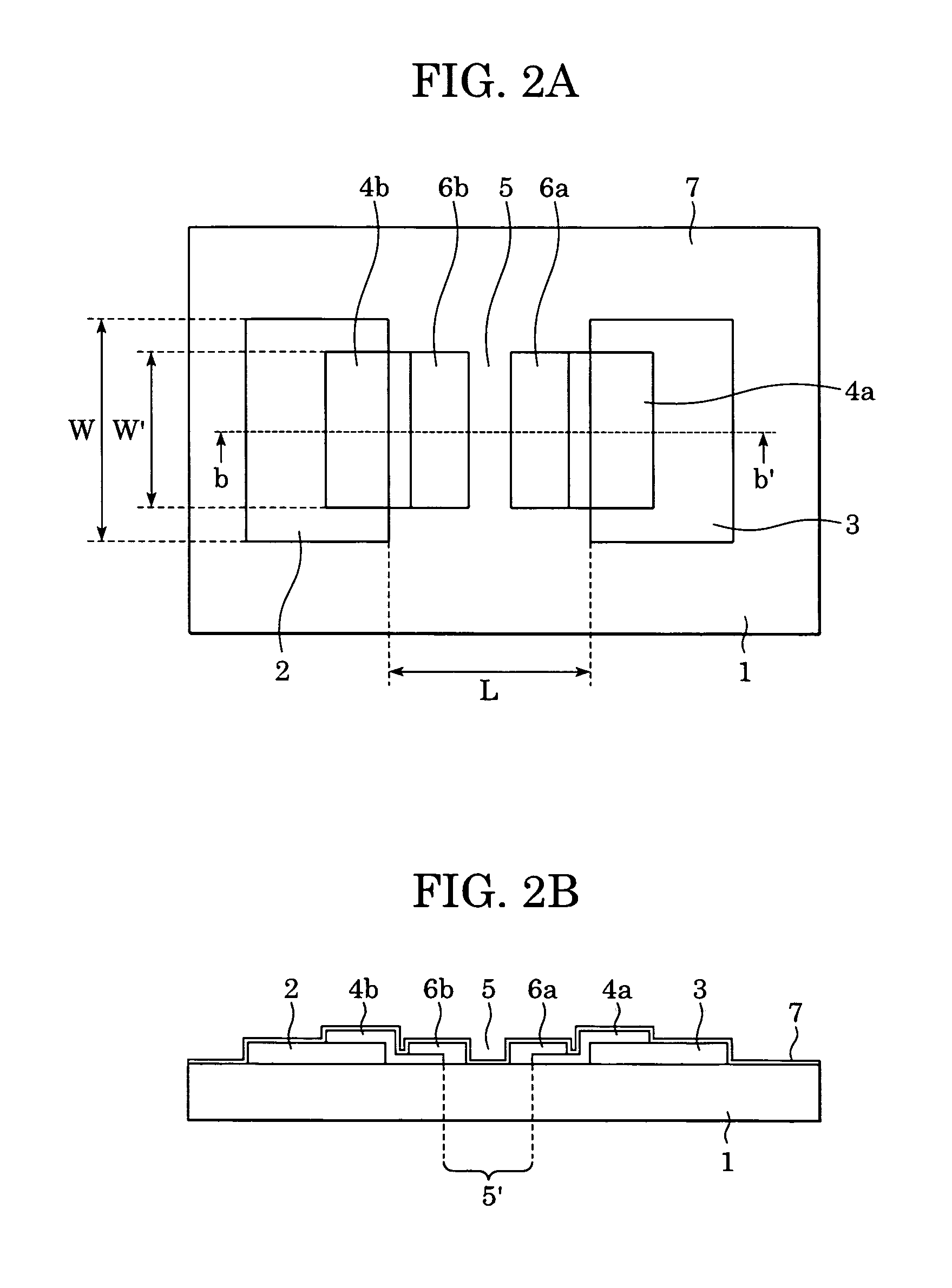
[0135]The electron-emitting device produced in Example 1 has the same structure as in FIGS. 2A and 2B. The process for manufacturing the electron-emitting device of the present example will be described with reference to FIGS. 2A, 2B, and 6A to 6E.

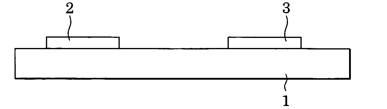
[0136]Step a: A silicon oxide layer was deposited to a thickness of 0.5 μm on a cleaned soda lime glass by sputtering. The resulting composite was used as the substrate 1. A host resist pattern was formed on the substrate 1, and subsequently a 5 nm thick Ti layer and a 100 nm thick Ni layer were deposited in that order by vacuum deposition. Then, the host resist pattern was dissolved in an organic solvent to form electrodes 2 and 3 by lift-off of the Ni and Ti deposition layers (FIG. 6A). The electrodes 2 and 3 had an interval L of 3 μm therebetween, and a width W of 300 μm.

[0137]Step b: A Cr mask was formed for forming a conductive film 4. Specifically, a 100 nm thick Cr layer was deposited on the substrate 1 having the electrode 2 and 3 ...

example 2

[0146]In Example 2, the carbon-containing gas tolunitrile used for the “activation” process in Example 1 was replaced with Hf[N(CH3)2]4 (tetrakis(dimethylamino)hafnium) gas. The partial pressure of the tetrakis(dimethylamino)hafnium gas was set at 1×10⁻⁴ Pa for the “activation” process.

[0147]The characteristics of the electron-emitting device after the “activation” process were examined. As a result, the electron-emitting device of the present example exhibited the same characteristics as those of the device produced by Steps a to e without Step f, but the emission current and electron emission efficiency were not increased, unlike the electron-emitting device of Example 1.

[0148]Then, after the “activation” process using tetrakis(dimethylamino)hafnium gas, the sequence of the following Steps A and B was repeated 50 cycles with the temperature of the substrate 1 maintained at 85° C.

[0149]Step A: H2O gas was introduced into the vacuum chamber until the pressure was increased to 3000 P...

example 3

[0153]In Example 3, the tetrakis(dimethylamino)hafnium used in Example 1 was replaced with Ti[N(CH3)2]4 (tetrakis(dimethylamino)titanium) and an electron-emitting device was produced. The characteristics of the resulting electron-emitting device were evaluated.

[0154]In the production process of the electron-emitting device in the present example, Steps a to e were performed in the same manner as in Example 1. Then, Step f was performed by repeating the sequence of the following Step A and Step B 100 cycles with the temperature of the substrate 1 maintained at 85° C.

[0155]Step A: H2O gas was introduced into the vacuum chamber until the pressure was increased to 1000 Pa, and the pressure was maintained for 10 seconds. Subsequently, the vacuum chamber was evacuated to a pressure of about 10 Pa.

[0156]Step B: Ti[N(CH3)2]4 (tetrakis(dimethylamino)titanium) gas was introduced into the vacuum chamber until the pressure was increased to 1000 Pa, and the pressure was maintained for 10 seconds...


PUM


Abstract

A method for manufacturing a precursor to an electron-emitting device includes the steps of preparing an electron-emitting member, and alternately exposing the electron-emitting member to an oxygen-containing gas and a metal-containing gas.

Description

BACKGROUND OF THE INVENTION[0001]1. Field of the Invention[0002]The present invention relates to a method for manufacturing an electron-emitting device, and to a method for manufacturing an electron source and an image display device using the electron-emitting device. The present invention also relates to an information displaying / reproducing apparatus using the image display device.[0003]2. Description of the Related Art[0004]An electron-emitting device may be classified into a field emission type or a surface conduction type.[0005]There is a case in which a surface of the electron-emitting device is coated with a metal film or a metal compound film to reduce the effective work function, increase the heat resistance (heat-proof), or stabilize the emission current, as disclosed in Japanese Patent Laid-Open Nos. 10-188778, 8-102247, 8-273523, and 9-102267. A plurality of the electron-emitting devices are arranged to define an electron source. The electron source is disposed so as to...

Claims


Application Information

Patent Timeline
Patent Type & Authority Patents(United States)
IPC IPC(8): H01J9/00H01J9/12H01J9/02H01J9/14
CPCH01J9/027
Inventor TAKEDA, TOSHIHIKONUKANOBU, KOKIMORIGUCHI, TAKUTO
Owner CANON KK
Why Eureka
Try Eureka