Magneto-resistance effect element and magnetic memory device

a technology of magnetic memory and resistance effect, which is applied in the manufacture of flux-sensitive heads, solid-state devices, instruments, etc., can solve the problems of insufficient lowering of writing current and increasing consumption power, and achieve low current, low consumption power, and high density

Inactive Publication Date: 2009-09-08
TOHOKU UNIV
View PDF15 Cites 33 Cited by
  • Summary
  • Abstract
  • Description
  • Claims
  • Application Information

AI Technical Summary

Benefits of technology

[0045]In accordance with the invention, a current including a resonance frequency component determined on the basis of magnetic domain wall potential is used as a current for moving a single magnetic domain wall. This allows the single magnetic domain wall to move with a low current at room temperature.
[0046]Moreover, applying a principle of the invention to a magnetic memory device allows a magnetic memory device, which is high in density and capable of writing with low current and low in consumption power, to be achieved.

Problems solved by technology

Accordingly, the consumption power increases and the Joule heat is generated, so that problems occur.
Such a current induction magnetic structure changing type MRAM has problems that necessity of a new mechanism for injecting a spin polarization electron into a free layer causes a complicated structure of a memory cell and that lowering in writing current is not always enough.

Method used


Image

  • Magneto-resistance effect element and magnetic memory device
  • Magneto-resistance effect element and magnetic memory device
  • Magneto-resistance effect element and magnetic memory device

Examples


embodiment 1

[0069]Now, a single magnetic domain wall resonance element in Embodiment 1 of the invention will be described, made reference to FIGS. 2 to 11.

[0070]Refer to FIG. 2.

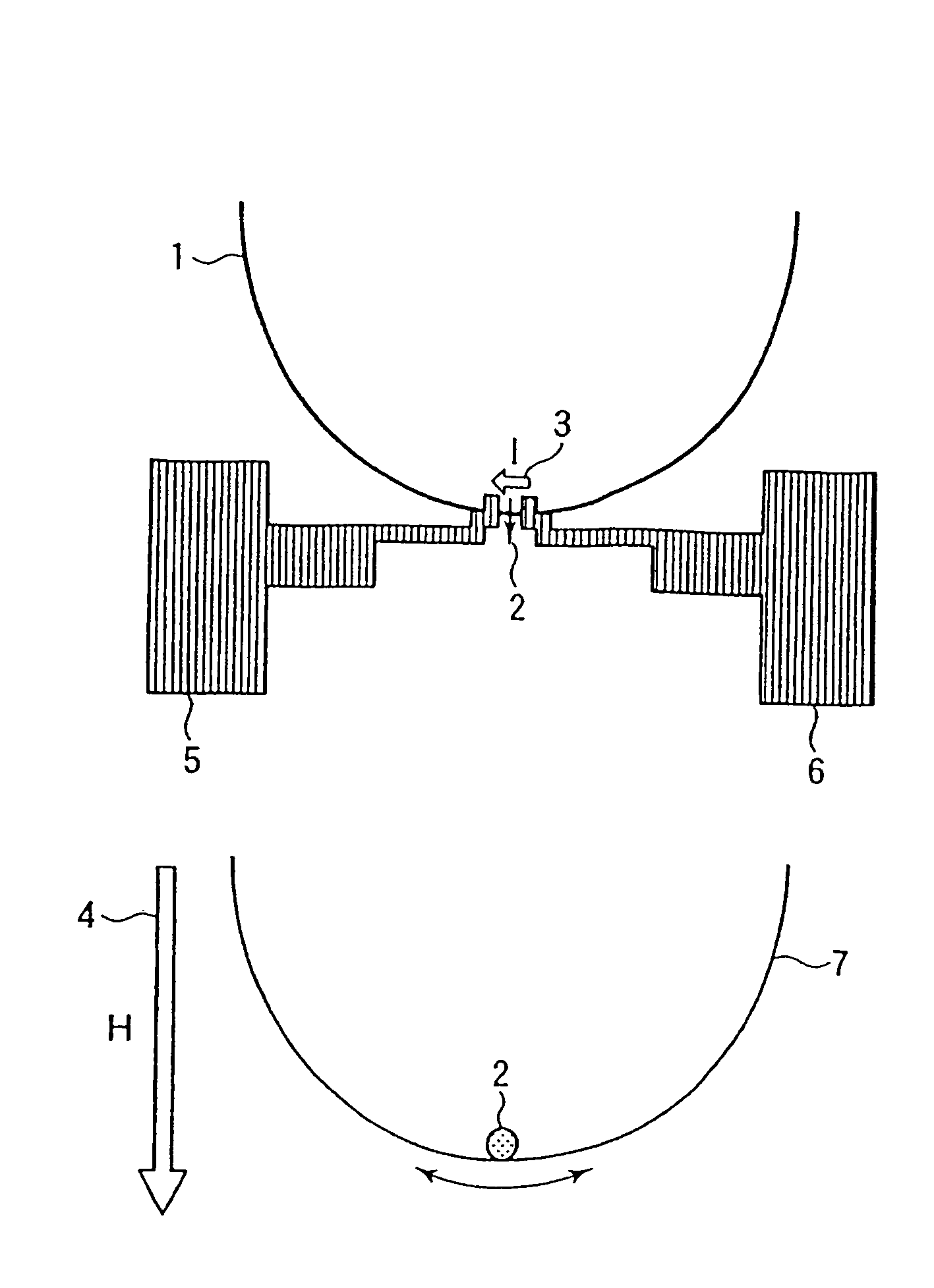
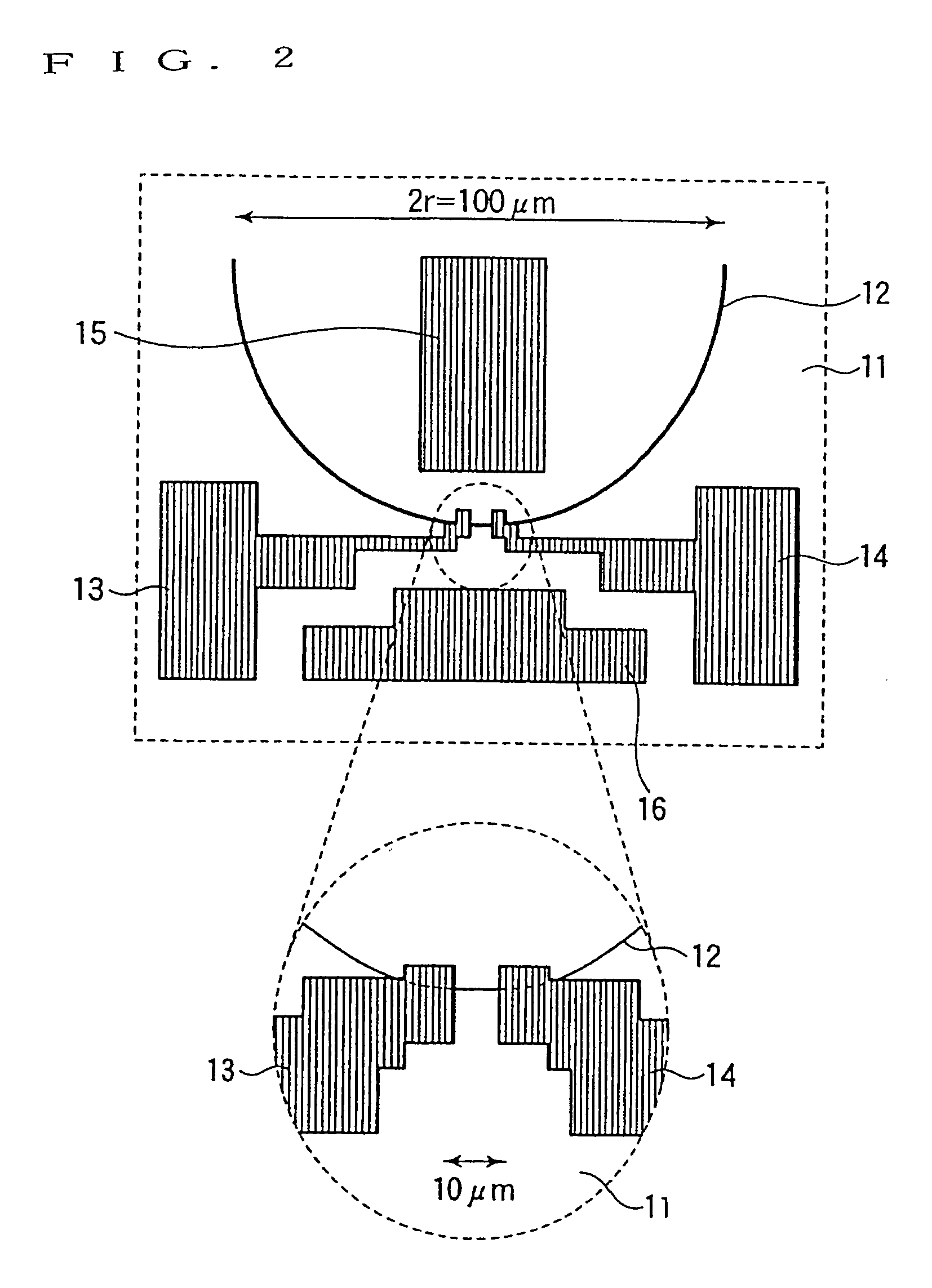
[0071]FIG. 2 is a plan view of a single magnetic domain wall resonance element in Embodiment 1 of the invention. In FIG. 2, a resist pattern (omitted from drawing) formed by electronic beam lithography is used as a lift-off pattern to form a film of a soft ferromagnet Ni81Fe10 into 45 nm in thickness, for example, by sputtering on a single crystal silicon substrate 11 whose surface is oxidized. The resist pattern is then removed to form a magnet loop 12 in the shape of a half arc, which is 70 nm in width and 50 μm in radius “r”, for example.

[0072]Following to the above, the sputtering film forming and a lift-off method are used again to form a pair of Cu electrodes 13 and 14 and to provide a pair of Cu earth electrodes 15 and 16 in a direction vertical to a direction that the pair of Cu electrodes 13 and 14 are opposed t...

embodiment 2

[0119]Now, described will be an MRAM in Embodiment 2 of the invention, made reference to FIGS. 12 to 14. The MRAM is a current induction magnetic domain wall moving type MRAM, which utilizes in writing data a phenomenon capable of moving the single magnetic domain wall with a low current by using high frequency current and by utilizing resonance, the phenomenon obtained from the result of Embodiment 1 described above. The external bound magnetic field H is not applied for the operation.

[0120]Refer to FIG. 12.

[0121]FIG. 12 is a schematic sectional view of an integral part of an MRAM in Embodiment 2 of the invention. In FIG. 12, a p-type well area 22 is first formed in a predetermined area of an n-type silicon substrate 21, the n-type silicon substrate 21 is selectively oxidized to form an element separation oxidation film 23, and then, a gate electrode made from WSi to be a sense line 25 for reading out is formed in an element forming area through a gate insulation film 24 to form an...

embodiment 3

[0145]Now, an MRAM in Embodiment 3 of the invention will be described, made reference to FIG. 17. In the MRAM, the two pinning parts of the MRAM in Embodiment 2 are formed not by ion injection but by introduction of a shape defect. Accordingly, described will be only a structure of the magnetic storage part.

[0146]Refer to FIG. 17.

[0147]FIG. 17 is a schematically perspective view of a magnetic storage part forming an MRAM in Embodiment 3 of the invention. In FIG. 17, narrow parts 51 and 52 are formed in two places of the Ni81Fe19 layer 41, which is to be used as a data writing layer, so as to be the pinning parts of the single magnetic domain wall 50.

[0148]The narrow parts 51 and 52 in the above case can be formed by selective etching after the film is formed or by means of a lift-off pattern shape. The degree of the narrow width can be determined so that the necessary magnetic domain wall potential can be achieved in accordance with a three-dimensional size of the Ni81Fe19 layer 41,...


PUM


Abstract

The invention relates to a magneto-resistance effect element and a magnetic memory device. Lowering the magnetic domain wall movement current and drive at room temperature in a current induction single magnetic domain wall movement phenomenon are achieved.A magneto-resistance effect element is formed by including at least: a magnet wire 1 for forming magnetic domain wall potential 7 binding a single magnetic domain wall 2; a magnetic field applying means for generating a magnetic field for introducing the single magnetic domain wall 2 into the magnet wire 1; and a drive current applying means for applying the current 3 including a resonance frequency component determined on the basis of the magnetic domain wall potential 7.

Description

TECHNICAL FIELD[0001]The present invention relates to a magneto-resistance effect element and a magnetic memory device, particularly, a magneto-resistance effect element and a magnetic memory device, which have a characteristic structure for carrying out movement of a single magnetic domain wall introduced into a magnetic material with the low current.BACKGROUND ART[0002]A magnetic sensor and a magnetic head, which utilize a magneto-resistance effect phenomenon that applying a magnetic field into a magnetic structure such as a spin valve structure causes a change in electric resistance, have been developed and used in practice.[0003]In recent years, noticed having been a magnetic random access memory (MRAM) using such a magneto-resistance effect. In the magnetic random access memory, the electric current is let flow into the magnetic structure to correspond to digital information of “0” or “1” by using a fact that the resistance value is changed in accordance with a direction of a s...

Claims


Application Information

Patent Timeline
Patent Type & Authority Patents(United States)
IPC IPC(8): G11C11/00G11C11/14G11C11/15
CPCB82Y25/00G01R33/093H01L43/08G11C11/16H01L27/228G11C11/1659G11C11/161G11C11/1673G11C11/1675G11C11/1657H10B61/22H10N50/10G11B5/39G11C11/15H10B99/00
Inventor SAITOH, EIJIMIYAJIMA, HIDEKI
Owner TOHOKU UNIV
Why Eureka
Try Eureka