Top-oxide-early process and array top oxide planarization

a top oxide and early process technology, applied in the field of manufacturing integrated circuits, can solve the problems of affecting the quality of integrated circuits, scratching of artifacts, etc., and achieves the effects of improving the quality and manufacturing yield of integrated circuits, enhancing manufacturing yield, and improving protection

Active Publication Date: 2009-10-13
GLOBALFOUNDRIES US INC
View PDF23 Cites 4 Cited by
  • Summary
  • Abstract
  • Description
  • Claims
  • Application Information

AI Technical Summary

Benefits of technology

[0009]It is therefore an object of the present invention to provide improved protection for differentiated areas of a chip during manufacture in combination with structures of reduced height of structures and reduced height difference between differentiated areas of the chip.
[0010]It is another object of the invention to provide a method for planarization of a chip surface and an array top oxide, in particular, having reduced susceptibility to engendering chip defects and improved manufacturing yield.
[0012]It is yet another object of the invention to provide an integrated circuit chip having a plurality of functional areas which can be fabricated with increased manufacturing yield and much reduced incidence of picture frame defects and foreign material faults.
[0015]The invention comprises a number of process features which provide improvements in integrated circuit quality and manufacturing yield and will be described in connection with three embodiments, each discussing features of the invention in preferred combinations and in connection with the preferred environment process for use of those features. As will be understood by those skilled in the art, these features of the invention may be used singly or in different combinations in regard to different processes (e.g. top oxide early (TOE), top oxide nitride (TON), top oxide late (TOL) and even more general processes such as planarization) to provide improved integrated circuits which can be manufactured with enhanced manufacturing yield. The first embodiment, illustrated in FIGS. 1-9, provides improvements over known TOE processes by using an optional support liner (nitride, polysilicon, etc.) with an oxide hard mask which provides improved protection for the support area and allows improved control over isolation trench structure height. (A TOE process with a support liner is disclosed in U.S. Pat. No. 6,620,677 to Hummler, which is hereby fully incorporated by reference.) A deglazing step prior to application of the liner and oxide hard mask reduces the average height of the array and support areas compared to the known TOE process. A polysilicon hard mask instead of the optional support liner and the oxide hard mask may also be used in accordance with the first embodiment of the invention for process simplification and improved control since a wet etch is required to remove oxide and nitride in the array area. Oxide and nitride in the array area can be easily removed with one polysilicon hard mask. Using one polysilicon hard mask, the step height difference between the array and support areas is less and array top oxide planarization is thus facilitated. The second embodiment of the invention, illustrated in FIGS. 1 and 10-14B provides a planarization technique which is an alternative to chemical / mechanical polishing (CMP) which provides improved planarity while avoiding artifacts associated with CMP and is particularly useful in TON processes which present particular problems for known planarization techniques. While the drawings illustrate this planarization process in connection with a TON process with which it is particularly advantageous, this planarization process can easily be applied to TOE and TOL processes as well. The third embodiment, which is illustrated in FIGS. 1, 3-5 and 16-22, employs etching to equalize step height in the array and support areas and provides substantial reduction of picture frame defects and foreign material faults, particularly in combination with the alternative planarization process of the second embodiment of the invention and in the environment of the first embodiment of the invention.

Problems solved by technology

The oxide formed over the array area is referred to as an array top oxide (ATO) and its formation is relatively critical since open or short failures can be caused by a slight lack of process control, the potential for capacitive coupling and the extremely close spacing of the capacitors and the word lines and bit lines which must be formed at a similarly close spacing.
Conversely, a process in which the nitride is removed in the array area with a block mask and the ATO is formed prior to removal of nitride in the support area is referred to as top-oxide-early (TOE) but has the disadvantage that relatively more masks are required than in the TOL and TON processes.
However, polishing processes such as CMP, while well-developed and mature, are imperfect and may cause several different types of undesirable artifacts.
One type of artifact is scratching which may occur due to a relatively larger grain of abrasive or a particle broken, chipped or abraded from the wafer being polished.
Scratching of insulator material and isolation structures may give rise to significant current leakage.
However, such a strategy may be incompatible with the process requirements for a particular design such as a top oxide nitride (TON) process used in memory chip manufacture alluded to above.
In modern integrated circuits and for an array top oxide structure, in particular, good uniformity and planarity within a tolerance of 15 nm is generally required and conventional CMP processes do not meet such a stringent specification due to scratches, dishing or other artifacts.
In summary, planarization, in general, and formation of ATO, including its planarization, in particular, is a major obstacle to obtaining acceptable manufacturing yield in high density integrated circuits having a plurality of functional areas.
Current known processes have not met required tolerances for planarity of ATO and defects due to scratching damage to circuit element structures, isolation structures and insulating material surfaces.

Method used


Image

  • Top-oxide-early process and array top oxide planarization
  • Top-oxide-early process and array top oxide planarization
  • Top-oxide-early process and array top oxide planarization

Examples


first embodiment

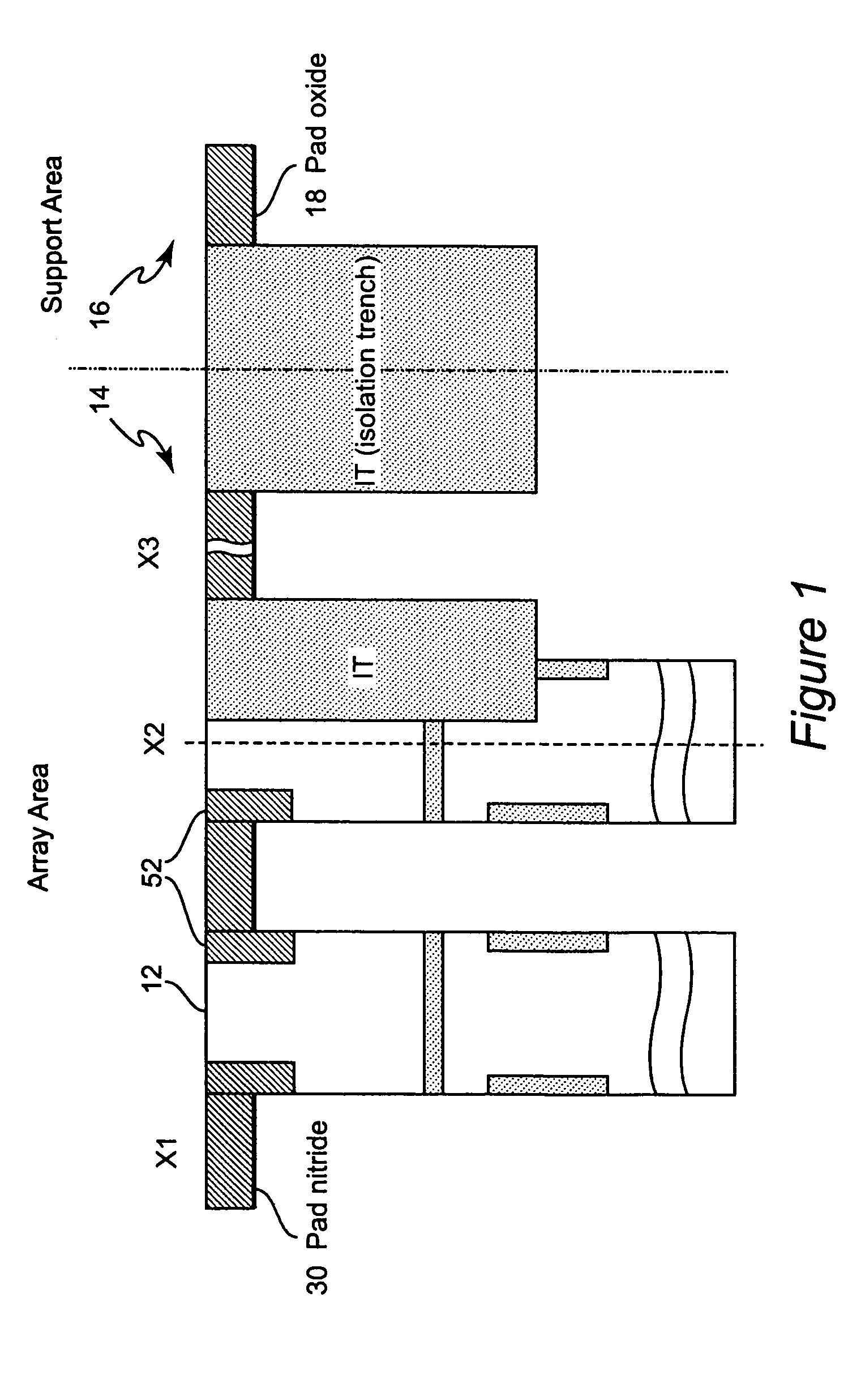
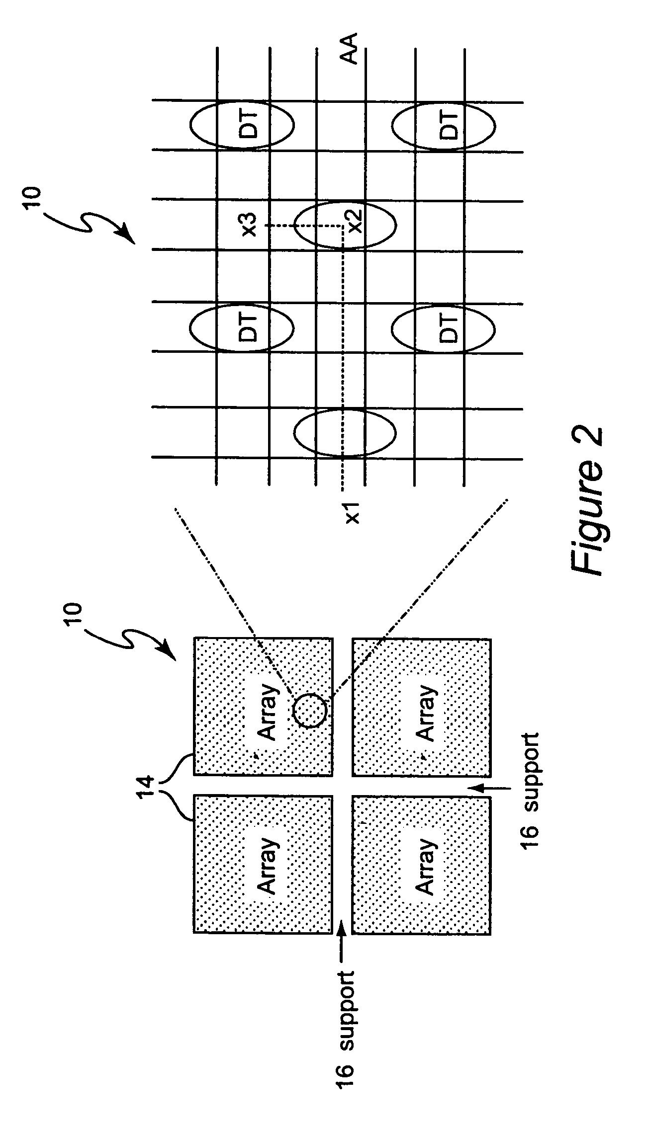
[0026]Referring now to FIGS. 3-7 application of the invention to the exemplary chip structure of FIGS. 1 and 2 in accordance with the invention will be discussed. FIG. 3 shows substantially the same chip cross-section shown in FIG. 1 except that a deglazing step has been performed which recesses isolation trench structures (IT) 32 at the top surfaces thereof below the level of the memory cell 12 studs and the pad nitride 30. Such a deglazing step prior to deposition of an oxide and nitride hard mask is desirable to control the step height of the array and support areas and, as such, constitutes a significant improvement over known TOE schemes. This deglaze sets the isolation trench (IT) heights in the array and support areas independently of subsequent array top oxide (ATO) processes and facilitates ATO planarization since the amount of materials to be removed is reduced. Additionally, an optional (isotropic) nitride liner 34 and an (isotropic) oxide hard mask 36 have been applied. ...

second embodiment

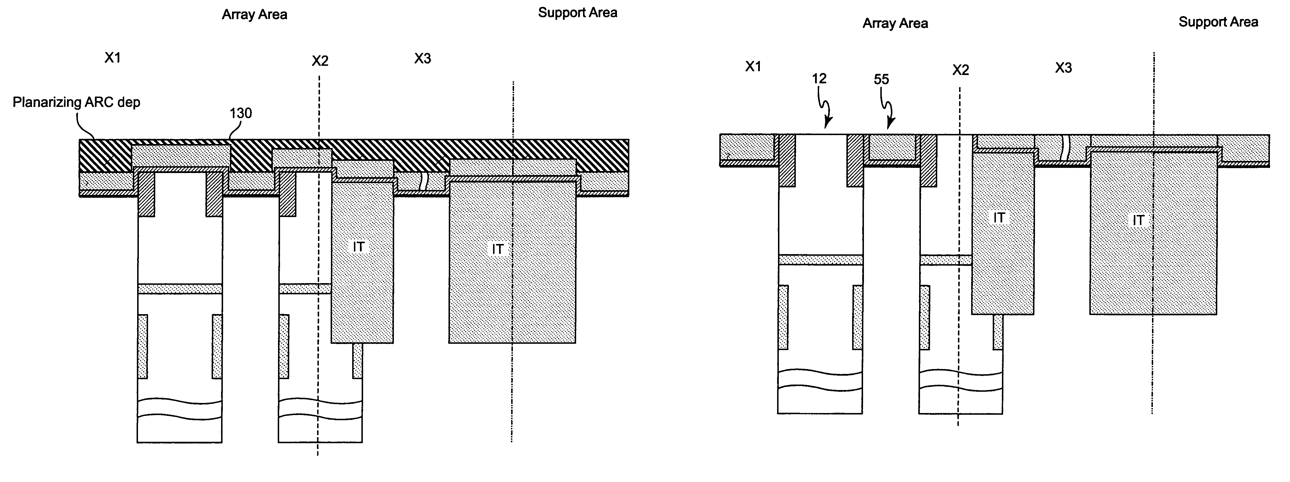
[0030]Referring now to FIG. 6, the ATO is planarized to or slightly into the ATO in active areas 55 such that the ATO is removed over the memory cells 12. As can be seen from a comparison with FIG. 5, the oxide hard mask is also removed from the support areas except where trench isolation structures were recessed in the deglazing process discussed above in regard to FIG. 3. Planarization can be performed by known CMP processes or by an ARC-assisted planarization process which will be discussed more fully in connection with the invention.

[0031]As shown in FIG. 7, a polysilicon hard mask layer 70 is deposited and a resist is applied and patterned to form a block-out mask 72. The polysilicon layer is then patterned in accordance with the block-out mask 72 to form a hard mask in the array area. Then, as shown in FIG. 8, the remaining oxide hard mask and support nitride liner in the support area are etched. The isolation trench oxide can also be etched to a desired height in the same pro...

third embodiment

[0048]Accordingly, the invention simultaneously avoids the engendering of defects of the picture frame and foreign material contamination types since deep etches are avoided while reliably removing planarization materials and avoiding damage to structures while achieving improved uniformity of planarity within a tolerance of under 15 nm in order to support high lithographic resolution for connection formation, bit line contact formation and other BEOL processes and which are particularly critical in the preferred environment of chips having both array and support areas, such as large capacity memories and logic processors having embedded memories.

[0049]The third embodiment of the invention features not only increased control over height of structures in the array and support areas by deglazing as discussed above in connection with FIG. 3 but adjusting the average height / step height of the structures to be substantially the same so that planarizing materials can adequately fill regio...


PUM


Abstract

Manufacturing yield of integrated circuits having differentiated areas such as array and support areas of a memory is improved by reducing height / step height difference between structures in the respective differentiated areas and is particularly effective in conjunction with top-oxide-early (TOE) and top-oxide-late processes. A novel planarization technique avoids damage of active devices, isolation structures and the like due to scratching, chipping or dishing which is particularly effective to improve manufacturing yield using TON processes and also using TOE and TOL processes when average height / step height is substantially equalized. Alternative mask materials such as polysilicon may also be used to simplify and / or improve control of processes.

Description

BACKGROUND OF INVENTION[0001]The present invention generally relates to the manufacture of integrated circuits and, more particularly, to the manufacture of integrated circuits having different functional areas requiring different processing and / or requiring planarizing processes.[0002]Increased density and proximity of both active and passive electronic device structures in an integrated circuit have been recognized to provide benefits in both performance and functionality of integrated circuits. For example, reduced lengths of signal propagation paths allow operation at higher clock rates while reducing susceptibility to noise. Increased numbers of devices on a single chip also generally support such improved performance while allowing a greater number and variety of circuit functions to be provided such as local voltage regulation and conversion, local memory and additional logic circuitry or coprocessors for microprocessors, non-volatile storage, redundant circuitry, self-test a...

Claims


Application Information

Patent Timeline
Patent Type & Authority Patents(United States)
IPC IPC(8): H01L21/3065H01L21/308H01L21/311
CPCH01L21/31053H01L27/10897H01L27/10894H01L27/10841H10B12/395H10B12/50H10B12/09
Inventor KIM, DEOK-KEEDIVAKARUNI, RAMACHANDRAAKATSU, HIROYUKIWORTH, GEORGESTRANE, JAYKIM, BYEONG
Owner GLOBALFOUNDRIES US INC
Why Eureka
Try Eureka