Apparatus and method for probing integrated circuits using laser illumination

a laser illumination and integrated circuit technology, applied in the direction of optical radiation measurement, light polarisation measurement, instruments, etc., can solve the problems of additional setup, difficult optimization of this algorithm, user burden, etc., and achieve the effect of high temporal resolution

Inactive Publication Date: 2009-11-10
DCG SYST
View PDF53 Cites 16 Cited by
  • Summary
  • Abstract
  • Description
  • Claims
  • Application Information

AI Technical Summary

Problems solved by technology

This is a burden to the user because it prevents the user from testing at arbitrary clock frequencies and it requires additional setup by the user.
Optimizing this algorithm is difficult.
From the economic perspective, the MLL is expensive, and custom electronics and software must be developed.
All these custom elements increase the complexity and the overall cost of the system.
A major difficulty encountered by all laser-base probe systems is deciphering the weak modulation in the reflected signal, which is caused by the response of the DUT to the stimulus.
Another difficulty is noise introduced into the signal by the DUT's vibrations.
However, the DUT interaction with the laser beam may cause changes mostly in the phase of the reflected laser beam, not its amplitude.
Consequently, the signal strength would be too weak for pure amplitude detection.
While this arrangement helps detect phase variations caused by the DUT, using this optical arrangement exposes the system to additional noise source from phase variations caused by DUT vibrations.
Also, alignment of reflected DUT and reference arm beams can be difficult.
Moreover, since the beam needs to be placed at various locations on the chip, the system needs to be designed so that the beam separation is adjustable, which complicates the optics design.
Differential detection isn't completely effective at eliminating vibrations because it is difficult to maintain proper balance of the two spatially separated detection arms.
In addition, the two return beams are not modulated identically by vibrations because they are not parked on identical structures.
Since the two beams traverse a common path, DUT vibrations largely modulate both identically, making this scheme inherently vibration insensitive.
However, the optics required to generate the delay are relatively complicated.
This can limit the maximum time span of a sampling window that can be used.

Method used


Image

  • Apparatus and method for probing integrated circuits using laser illumination
  • Apparatus and method for probing integrated circuits using laser illumination
  • Apparatus and method for probing integrated circuits using laser illumination

Examples


Embodiment Construction

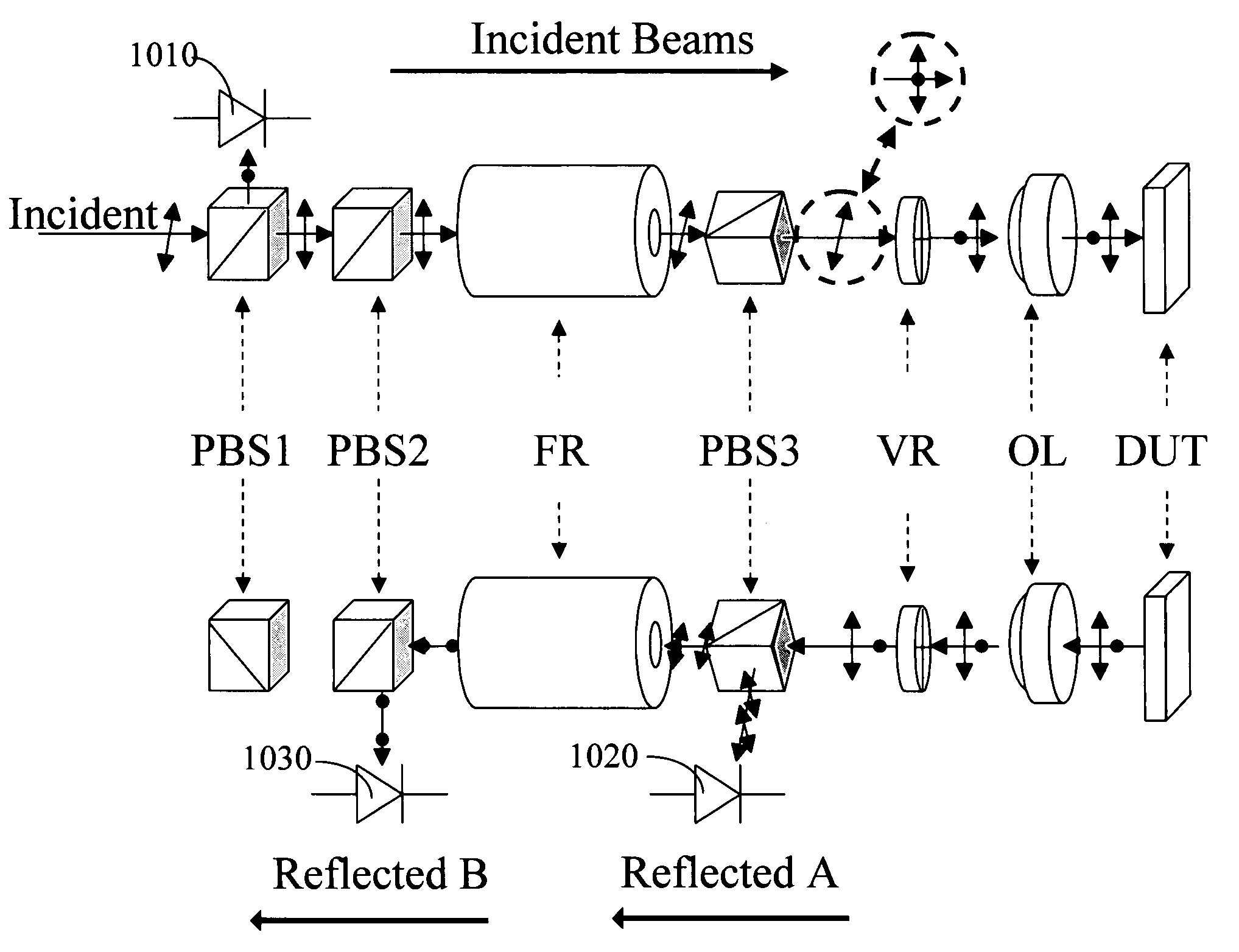
[0043]An embodiment of the invention will now be described in details with reference to FIG. 6 and, for illustration purposes, it will be depicted in a manner highlighting differences from the system of FIG. 1. Most notably, in this embodiment of the invention a continuous wave (CW) laser source is used, rather than the pulsed laser source. Using a CW laser source reduces the overall cost and complexity of the system. Of course, as noted above, for laser probing of today's integrated circuits a high temporal resolution is needed, which led to the use of mode-locked lasers. In this embodiment, however, the CW laser is used in conjunction with a very wide bandwidth differential amplifier and a data acquisition arrangement to achieve the desired temporal resolution. Additionally, the system is capable of providing other information that does not necessitate temporal resolution. Other major differences include pointing the reference and the probing beam as the same location on the DUT, ...


PUM


Abstract

An apparatus and method for laser probing of a DUT at very high temporal resolution is disclosed. The system includes a CW laser source, a beam optics designed to point two orthogonally polarized beams at the same location on the DUT, optical detectors for detecting the reflected beams, collection electronics, and an oscilloscope. The beam optics defines a common-path polarization differential probing (PDP) optics. The common-path PDP optics divides the laser beam into two beams of orthogonal polarization. Due to the intrinsic asymmetry of a CMOS transistor, the interaction of the beams with the DUT result in different phase modulation in each beam. This difference can be investigated to study the response of the DUT to the stimulus signal.

Description

BACKGROUND[0001]1. Field of the Invention[0002]The present invention relates to an apparatus and method for probing integrated circuits using laser illumination.[0003]2. Description of the Related Art[0004]Probing systems have been used in the art for testing and debugging integrated circuit (IC) designs and layouts. Various laser-based systems for probing IC's are known in the prior art. While some description of the prior art is provided herein, the reader is encouraged to also review U.S. Pat. Nos. 5,208,648, 5,220,403 and 5,940,545, which are incorporated herein by reference in their entirety. Additional related information can be found in Soref, R. A. and B. R. Bennett, Electrooptical Effects in Silicon. IEEE Journal of Quantum Electronics, 1987. QE-23(1): p. 123-9; Kasapi, S., et al., Laser Beam Backside Probing of CMOS Integrated Circuits. Microelectronics Reliability, 1999. 39: p. 957; Wilsher, K., et al. Integrated Circuit Waveform Probing Using Optical Phase Shift Detectio...

Claims


Application Information

Patent Timeline
Patent Type & Authority Patents(United States)
IPC IPC(8): G01B11/00
CPCG01R31/308G01R31/311
Inventor KASAPI, STEVENWILSHER, KENNETHWOODS, GARYLO, WILLIAMISPASOIU, RADUNATARAJ, NAGAMANIBOIADJIEVA, NINA
Owner DCG SYST
Why Eureka
Try Eureka