Wurtzite thin film, laminate containing wurtzite crystalline layer and their manufacturing methods

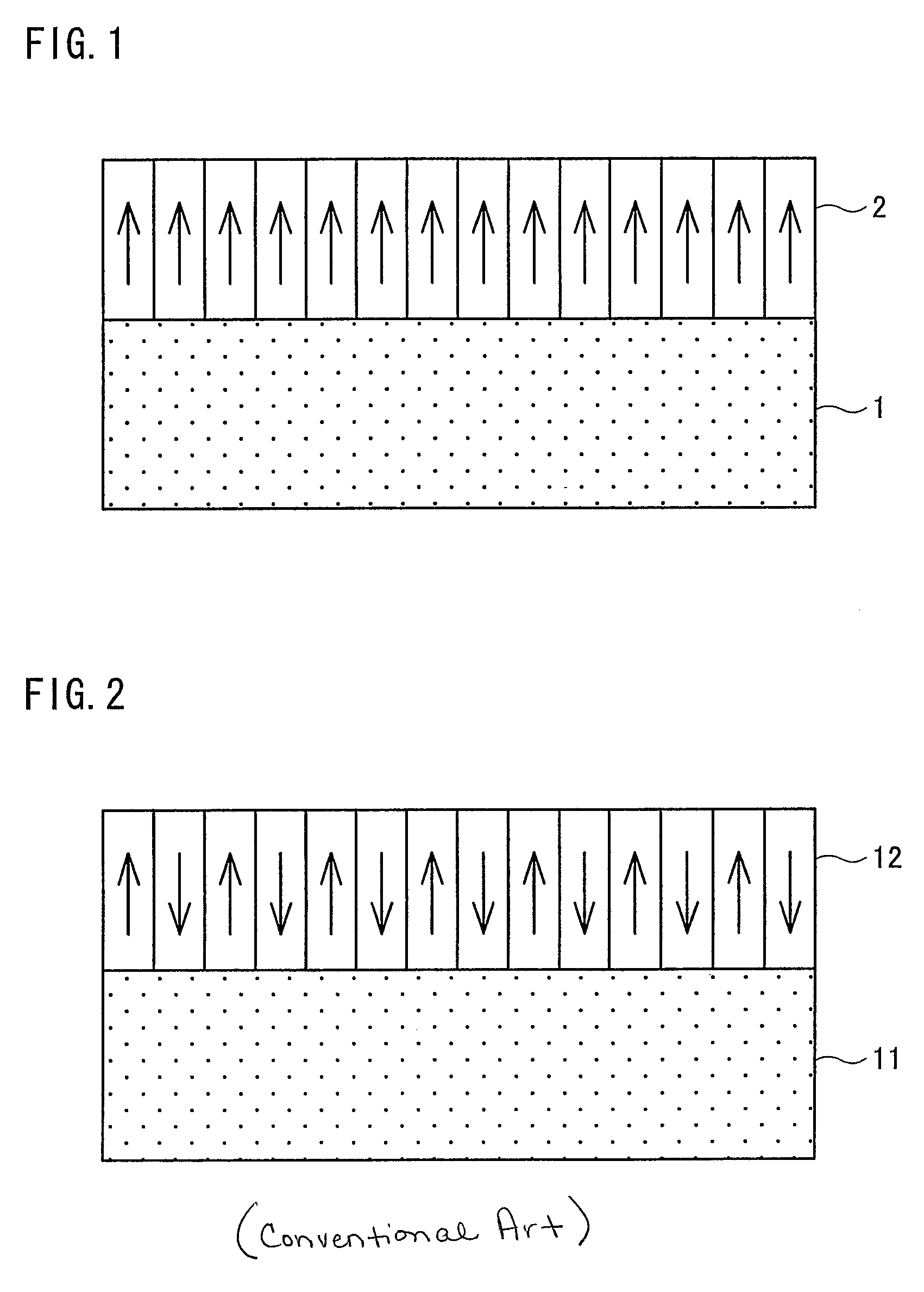
a technology of wurtzite and crystalline layer, which is applied in the direction of generator/motor, crystal growth process, polycrystalline material growth, etc., can solve the problems of reducing the overall piezoelectric effect, difficult to control the crystallinity and crystalline orientation of the wurtzite crystalline structure compound, and the study of polarization has not been made until now. , to achieve the effect of effective piezoelectric property and effective piezoelectric property

Active Publication Date: 2010-01-05
NAT INST OF ADVANCED IND SCI & TECH
View PDF14 Cites 26 Cited by
  • Summary
  • Abstract
  • Description
  • Claims
  • Application Information

AI Technical Summary

Benefits of technology

[0028]In addition, as a result of diligent studies in view of the above problems, the present inventors found out that it is possible to improve the crystallinity and crystalline orientation of the second wurtzite crystalline layer by (i) forming in advance the first wurtzite crystalline layer under the functional material layer that is a ground, that is, between the substrate and the functional material layer and then (ii) forming the second wurtzite crystalline layer on the functional material layer. This finding has led to the completion of the present invention.
[0032]In the case of using as the electronic component material the thin film made of the wurtzite structure compound, it is important to form the thin film so that the polarization directions of the crystal grains are adequately aligned in a uniform direction. In this way, the thin film can obtain the effective piezoelectric property. Note that the polarization directions are adequately aligned in a uniform direction when the polarizability of the crystal grains is 51% or more.
[0033]As described above, the polarizability of the crystal grains in the wurtzite thin film of the present invention is 51% or more, that is, the wurtzite thin film of the present invention has the adequate polarizability to obtain the effective piezoelectric property. Therefore, the wurtzite thin film of the present invention can be effectively utilized for various electronic components as the electronic component material having the piezoelectric property.
[0037]According to the above method, the polarizability of the crystal grains in the wurtzite thin film is 51% or more. That is, it is possible to manufacture the wurtzite thin film having an adequate polarizability to obtain the effective piezoelectric property. Therefore, the wurtzite thin film manufactured by the method of the present invention can be effectively utilized for various electronic components as the electronic component material having the piezoelectric property.
[0046]In the method for manufacturing the wurtzite thin film in accordance with the present invention, it is possible to further improve the polarizability of the crystal grains in the wurtzite thin film by adopting the above-descried film-forming conditions. Therefore, it is possible to manufacture the wurtzite thin film which has much better piezoelectric property and is more useful as the electronic component material.
[0059]With the above structure or method, it is possible to manufacture the laminate having the multilayer structure in which the wurtzite crystalline layer whose crystallinity and crystalline orientation are satisfactory and the functional material layer are complexed with each other regardless of the crystalline structure of the functional material layer. Therefore, it is possible to improve the quality of the electronic component material made by complexing the wurtzite crystalline structure compound with the functional material having conductivity, etc.

Problems solved by technology

This is because crystal grains polarized in opposite directions decrease the overall piezoelectric effect.
Therefore, studies of the polarization have not been made until now.
However, in the case of forming the layer made of the wurtzite crystalline structure compound on the functional material layer that is a ground, there is a problem in that it is difficult to control the crystallinity and crystalline orientation of the wurtzite crystalline structure compound.
However, in the case of forming the second wurtzite crystalline compound layer on the functional material layer which not partially but entirely covers the first wurtzite crystalline compound layer, there are problems in that an internal stress of the functional material layer is large and the second wurtzite crystalline structure compound layer is easily peeled off.
Moreover, in the case in which the functional material layer is made of a metal having a body-centered cubic structure or a hexagonal close-packed lattice structure, the control of the crystallinity and crystalline orientation of the wurtzite crystalline layer formed on the functional material layer is more difficult than that in the case in which the functional material layer is made of a material having the face-centered cubic structure, and actually a method for controlling these has not been found so far.

Method used


Image

  • Wurtzite thin film, laminate containing wurtzite crystalline layer and their manufacturing methods
  • Wurtzite thin film, laminate containing wurtzite crystalline layer and their manufacturing methods
  • Wurtzite thin film, laminate containing wurtzite crystalline layer and their manufacturing methods

Examples


example 1

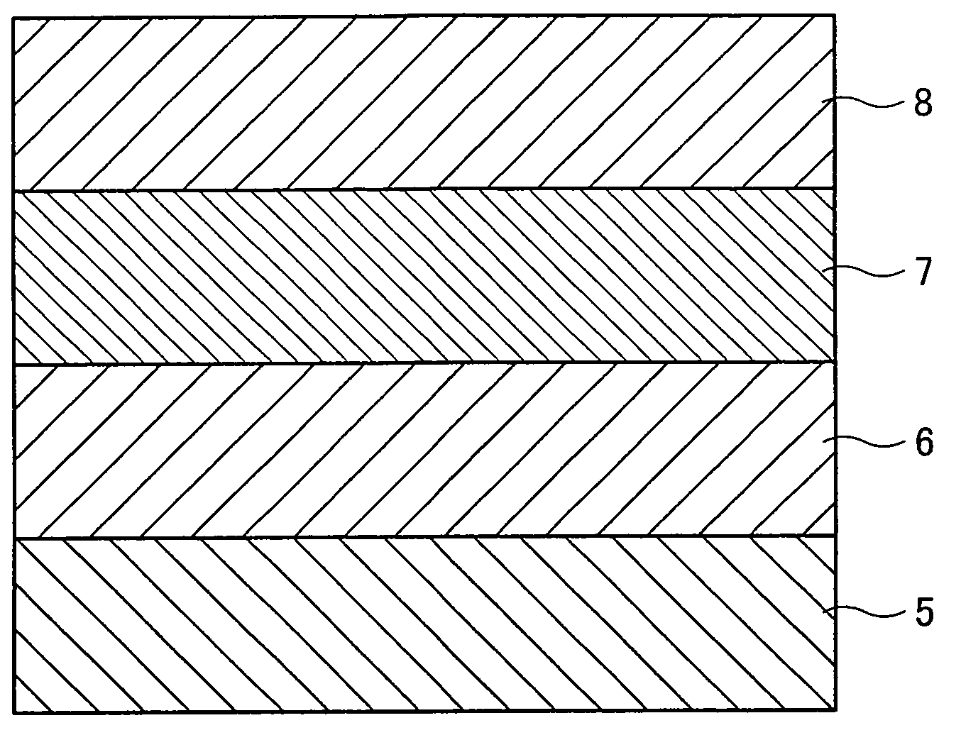
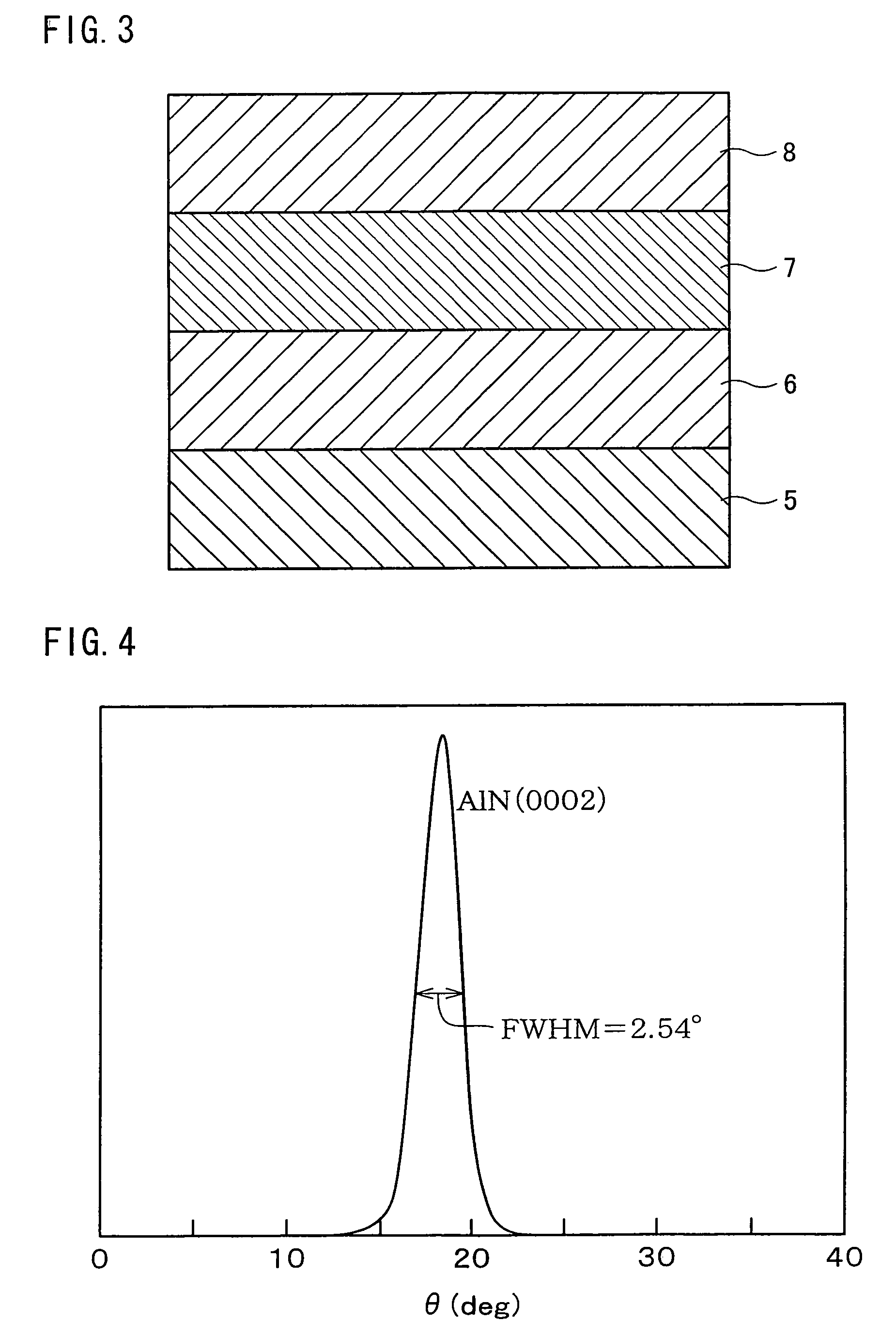
[0136]In Example 1, AlN was used as the wurtzite structure compound so as to form a wurtzite thin film on a substrate. The film-forming conditions are as follows: The substrate temperature was 400° C., the nitrogen concentration was 50%, the high-frequency power density was 7.83 W / cm2 and the sputtering pressure was 0.5 Pa. Under these film-forming conditions, the wurtzite thin film was formed on the substrate so that the film thickness of AlN (aluminum nitride) was 1 μm. The polarizability of the wurtzite thin film obtained here was measured and was about 80%, that is, the measurement confirmed that the wurtzite thin film had an adequate polarizability to obtain an effective piezoelectric property.

example 2

[0137]Aluminum nitride (AlN) as the first wurtzite crystalline structure compound, molybdenum (Mo) as the functional material and aluminum nitride (AlN) as the second wurtzite crystalline structure compound were formed on an Si monocrystalline substrate by RF magnetron sputtering. The films of the first and second aluminum nitride were formed under the following conditions: Metal aluminum (Al) was used as a target; argon (Ar) and nitrogen (N2) were used as reactive gas; the substrate temperature was 300° C.; and an RF output was 400 W. Moreover, the film of molybdenum (Mo) was formed under the following conditions: Metal molybdenum (Mo) was used as a target; argon (Ar) was used as reactive gas; no heat was applied; and an RF output was 100 W.

[0138]The films were formed so that the film of the first aluminum nitride (AlN) had the thickness of 100 nm, the film of molybdenum (Mo) had the thickness of 200 nm and the film of the second aluminum nitride (AlN) had the thickness of 1 μm.

[01...


PUM

PropertyMeasurementUnit
thicknessaaaaaaaaaa
thicknessaaaaaaaaaa
Curie pointaaaaaaaaaa

Abstract

A thin film made of a wurtzite structure compound is manufactured by a reactive sputtering using a metal material as a target, and a nitrogen gas or oxygen gas as a reactive gas. By optimizing film-forming conditions when manufacturing the film, it is possible to obtain a wurtzite thin film whose polarization directions of crystal grains are aligned in a uniform direction. There is provided a laminate including a first wurtzite crystalline layer made of a wurtzite crystalline structure compound is formed in advance between a substrate and a functional material layer that is a ground. Thus it is possible to improve the crystallinity and crystalline orientation of a second wurtzite crystalline layer on the functional material layer.

Description

TECHNICAL FIELD[0001]The present invention relates to a wurtzite thin film whose crystalline orientation is satisfactory and polarization directions are aligned in a uniform direction, a laminate containing a wurtzite crystalline layer, and their manufacturing methods.BACKGROUND ART[0002]A semiconductor made of a wurtzite structure compound, such as aluminum nitride (AlN), has a piezoelectric property and a pyroelectric property. Since the wurtzite structure compound has such properties, the wurtzite structure compound is applicable to various devices, such as electronic devices, optical devices and high-pressure proof / high-temperature proof electronic devices.[0003]In fact, the wurtzite structure compound has been applied as a material for various electronic components, such as high-frequency oscillators, filters for high frequency, various sensors, switches, ultrasonic oscillators, electromechanical transducers for audible bandwidth and light emitting elements.[0004]Among the wurt...

Claims


Application Information

Patent Timeline
Patent Type & Authority Patents(United States)
IPC IPC(8): H01L41/083C23C14/06C30B23/00H01L41/257H01L41/316
CPCC23C14/06C30B23/00C30B29/403C30B29/406H01L41/316H01L41/257H10N30/045H10N30/076
Inventor AKIYAMA, MORITOUENO, NAOHIROTATEYAMA, HIROSHIKAMOHARA, TOSHIHIRO
Owner NAT INST OF ADVANCED IND SCI & TECH
Why Eureka
Try Eureka