
Electrolytic processing apparatus and method

a processing apparatus and electrolysis technology, applied in the direction of electric circuits, manufacturing tools, electric circuits, etc., can solve the problems of reducing the performance of dielectric materials, affecting the processing efficiency of dielectric materials, and affecting the quality of dielectric materials, so as to improve the uniform processing rate and improve the evenness of the processed surfa

Inactive Publication Date: 2010-02-02
EBARA CORP
View PDF23 Cites 2 Cited by
  • Summary
  • Abstract
  • Description
  • Claims
  • Application Information

AI Technical Summary

Benefits of technology

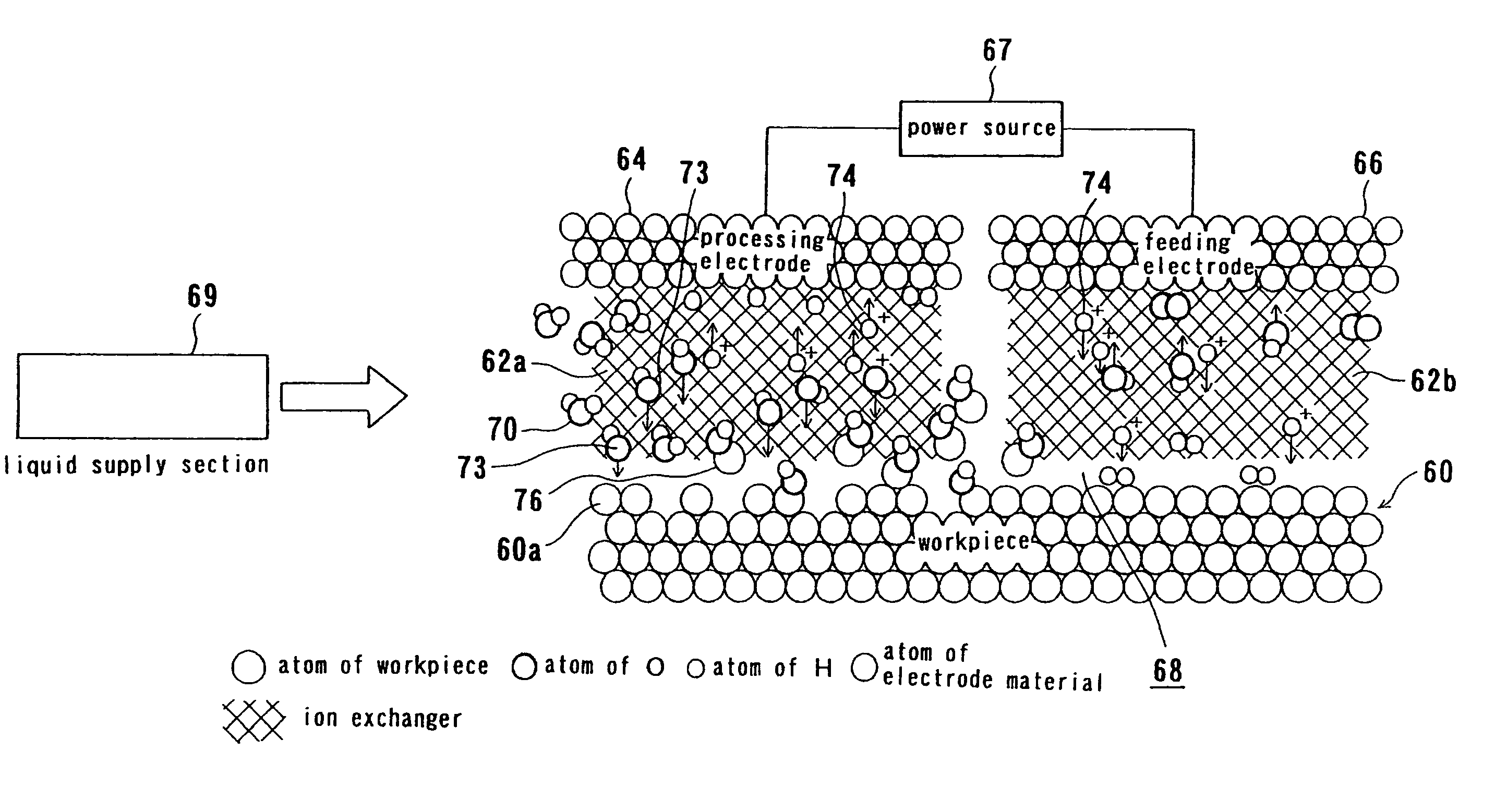
"The present invention provides an electrolytic processing apparatus and method that can control the processing rate distribution over the entire surface of a workpiece, improving uniformity of the processing rate and evenness of the processed surface. This is achieved by using an ion exchanger and applying a voltage to each of the divided electrode parts, allowing for independent control of voltage and electric current for each part. The apparatus can also process a conductive material formed on the surface of a substrate or remove extraneous matter from the surface of a workpiece, without the need for a CMP treatment. The use of a divided electrode structure and independent control of voltage and electric current for each part makes the apparatus more efficient and flexible. The fluid supply section can use ultrapure water or a liquid with low electric conductivity to carry out a clean processing without leaving impurities on the surface of a workpiece. The apparatus can also apply different constant voltages to different parts of the divided electrodes to control the end point of processing. Overall, the invention provides an improved electrolytic processing method and apparatus that can control the processing rate distribution and improve uniformity of the processed surface."

Problems solved by technology

Under these circumstances, in such a conventional machining method that a desired portion in a workpiece is physically destroyed and removed from the surface thereof by a tool, a large number of defects may be produced to deteriorate the properties of the workpiece.
As a result, a ruthenium film is formed also in the peripheral region of the substrate and, in addition, the back surface of the substrate is unavoidably contaminated with ruthenium.
The ruthenium film formed on or adhering to the peripheral region or back surface of a substrate, i.e. the non-circuit region of the substrate, is not only unnecessary, but can also cause cross-contamination during later transfer, storage and various processing steps of the substrate whereby, for instance, the performance of a dielectric material can be lowered.
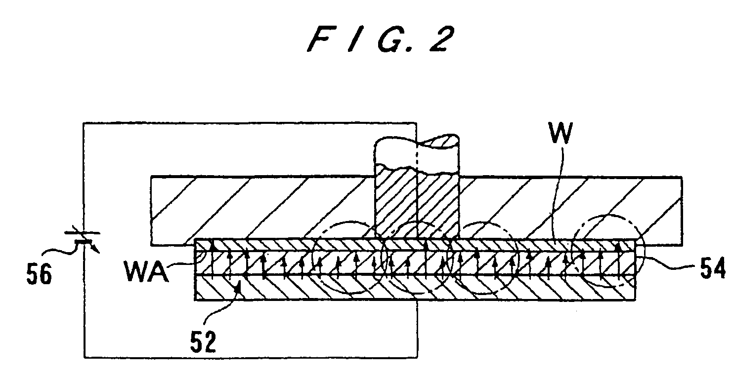
According to the conventional electrolytic processing apparatus as shown in FIG. 2, however, because of unevenness of the electric current value due to the shape of the processing electrode 52 or to the influence of the reaction products or gas bubbles generated during processing, the processing rate is likely to be uneven in the to-be-processed surface WA.
On the other hand, chemical mechanical polishing (CMP), for example, generally necessitates a complicated operation and control, and needs a considerably long processing time.
This also imposes a considerable load on the slurry or cleaning liquid waste disposal.
Also in this connection, it is to be pointed out that though a low-k material, which has a low dielectric constant, is expected to be predominantly used in the future as a material for the insulating film of a semiconductor substrate, the low-k material has a low mechanical strength and therefore is hard to endure the stress applied during CMP processing.
According to this method, the mechanical processing is carried out to the growing surface of a plating film, causing the problem of denaturing of the resulting film.
Further, though it is desired that an ion exchange for use in electrolytic processing be tightly fixed on the exposed surface of a processing electrode or a feeding electrode, as described above, in order to ensure evenness of the processing accuracy, it has practically been difficult to keep the ion exchanger fixed tightly on the electrode.
Thus, when continuing electrolytic processing while an ion exchanger is fixed on an electrode by screwing or with an adhesive tape, the fixing of ion exchanger is likely to become incomplete, so that the ion exchanger can move easily, impairing evenness of the processing accuracy.

Method used


Image

  • Electrolytic processing apparatus and method
  • Electrolytic processing apparatus and method
  • Electrolytic processing apparatus and method

Examples


first embodiment

[0134]FIG. 7 is a partly sectional block diagram schematically showing an electrolytic processing apparatus 50 according to the present invention. The electrolytic processing apparatus 50 comprises an electrode holder 12 for holding a processing electrode 18 as an electrode, an electrode-rotating shaft 13 mounted to the electrode holder 12, a substrate holder 14, provided above the electrode holder 12, for attracting and holding a substrate W as a workpiece or as a feeding electrode, and a substrate-rotating shaft 15 mounted to the substrate holder 14. According to this embodiment, the substrate W functions as a feeding electrode. The electrolytic processing apparatus 50 further includes a power source 23 for applying a voltage or an electric current between the processing electrode 18 and the substrate W, as will be described hereinbelow.

[0135]The electrolytic processing apparatus 50 is also provided with a hollow motor 41 as a substrate-rotating means for rotating the substrate ho...

second embodiment

[0156]FIG. 10 is a partly sectional block diagram schematically showing an electrolytic processing apparatus 50a according to the present invention.

[0157]According to the electrolytic processing apparatus 50a, a processing electrode 118 and a feeding electrode 136 are held by an electrode holder 112. The processing electrode 118 is divided into five processing electrode parts 118-1 through 118-5 by four ring-shaped insulators 140-1 through 140-4, and is peripherally surrounded by a ring-shaped insulator 140-5. In the processing electrode parts 118-1 through 118-5, a number of through-holes 129 are formed as a fluid supply section for supplying an electrolytic solution 102 to the substrate W (one through-hole 129 for each of the processing electrode parts 118-1 through 118-5 is depicted in FIG. 10).

[0158]The outermost insulator 140-5 is surrounded by a ring-shaped feeding electrode 136. The whole processing electrode parts 118-1 through 118-5, the whole insulators 140-1 through 140-5...

fourth embodiment

[0175]FIG. 17 is a vertical sectional view schematically showing the electrolytic processing apparatus 334 according to the present invention. As shown in FIG. 17, the electrolytic processing apparatus 334 includes a pivot arm 340 that can pivot horizontally and move vertically, a substrate holder 342, supported at the free end of the pivot arm 340, for attracting and holding the substrate W with its front surface facing downward (face-down), a disk-shaped electrode section 344 positioned beneath the substrate holder 342, and a power source 346 connected to the electrode section 344. In this embodiment, the size of the electrode section 344 is designed to have a slightly larger diameter than the diameter of the substrate W to be held by the substrate holder 342.

[0176]The pivot arm 340, which pivots horizontally by the actuation of a motor 348 for pivoting, is connected to the upper end of a pivot shaft 350. The pivot shaft 350, which moves up and down integrated with the pivot arm 3...


PUM

PropertyMeasurementUnit
electric conductivityaaaaaaaaaa

Abstract

This invention relates to an electrolytic processing apparatus and method useful for processing a conductive material formed in the surface of a substrate, or for removing impurities adhering to the surface of a substrate. An electrolytic processing apparatus, including, a processing electrode that can come close to a workpiece, a feeding electrode for feeding electricity to the workpiece, an ion exchanger disposed in the space between the workpiece and the processing and the feeding electrodes, a fluid supply section for supplying a fluid between the workpiece and the ion exchanger, and a power source. The processing electrode and / or the feeding electrode is electrically divided into a plurality of parts, and the power source applies a voltage to each of the divided electrode parts and can control voltage and / or electric current independently for each of the divided electrode parts.

Description

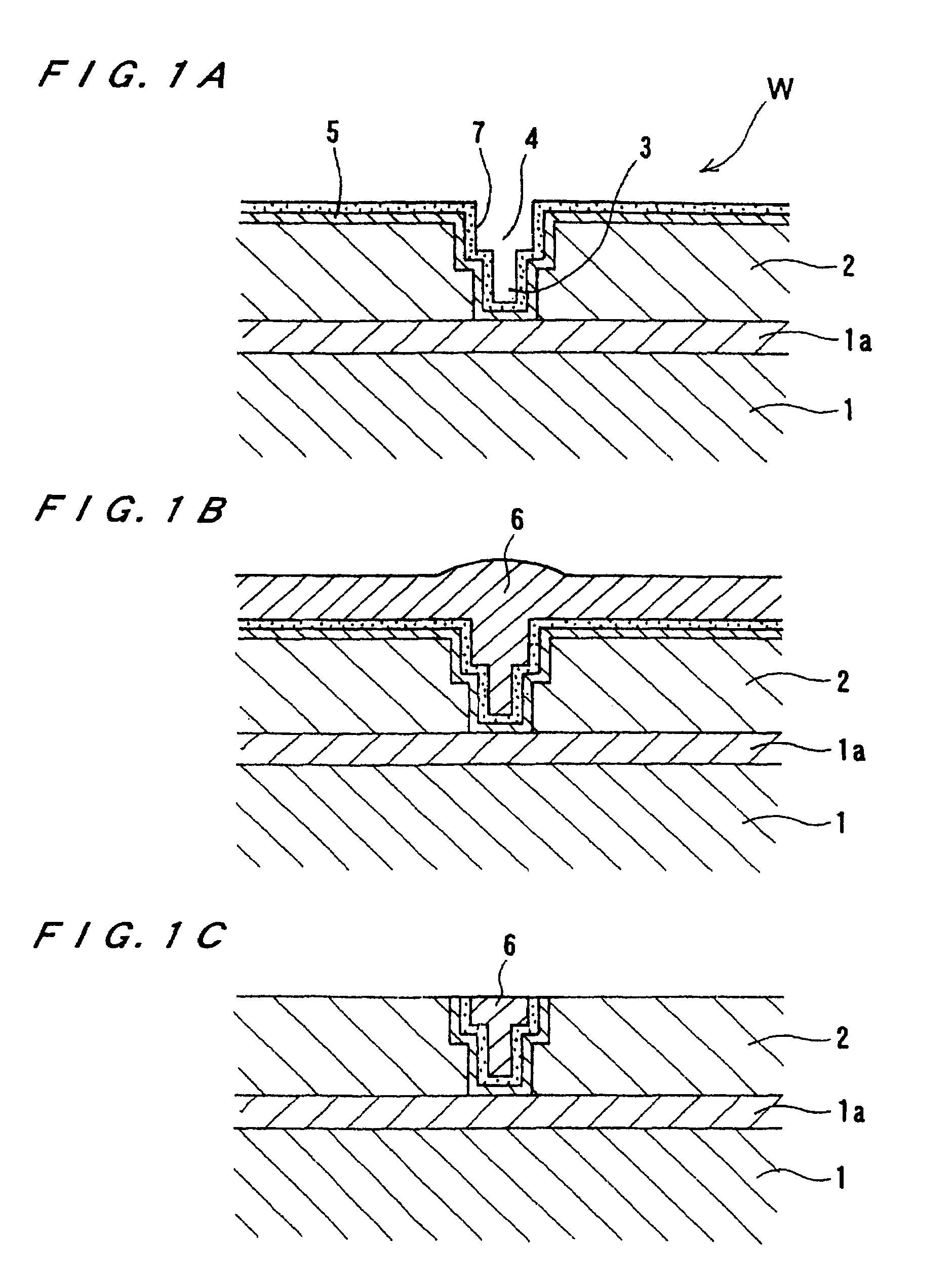
TECHNICAL FIELD[0001]This invention relates to an electrolytic processing apparatus and method, and more particularly to an electrolytic processing apparatus and method useful for processing a conductive material formed in the surface of a substrate, especially a semiconductor wafer, or for removing impurities adhering to the surface of a substrate.[0002]The present invention also relates to a fixing method and structure for an ion exchanger for use in electrolytic processing for processing a conductive material in the surface of a substrate, such as a semiconductor wafer, or removing impurities adhering to the surface of the substrate, and further relates to an electrolytic processing apparatus which is provided with the ion exchanger-fixing structure.BACKGROUND ART[0003]In recent years, instead of using aluminum or aluminum alloys as a material for forming interconnection circuits on a substrate such as a semiconductor wafer, there is an eminent movement towards using copper (Cu) ...

Claims


Application Information

Patent Timeline
Patent Type & Authority Patents(United States)
IPC IPC(8): C25F3/16C25F7/00C25F3/00H01L21/3063H01L21/3213
CPCC25F3/00C25F7/00H01L21/32134H01L21/3063B23H3/02
Inventor SHIRAKASHI, MITSUHIKOKUMEKAWA, MASAYUKIYASUDA, HOZUMIKOBATA, ITSUKINABEYA, OSAMU
Owner EBARA CORP
Learn More