Deposition method for a transition-metal-containing dielectric

a dielectric and transition metal technology, applied in the direction of fixed capacitor details, thin/thick film capacitors, coatings, etc., can solve the problem of short retention time and achieve the effect of stabilizing the amorphous

Inactive Publication Date: 2010-02-23
POLARIS INNOVATIONS LTD
View PDF9 Cites 18 Cited by
  • Summary
  • Abstract
  • Description
  • Claims
  • Application Information

AI Technical Summary

Benefits of technology

[0014]One advantage of the above method is to provide a clean transition metal containing material layer, in particular a transition metal oxide containing layer, on a substrate and to inhibit the formation of a substrate oxide. Therefore, a later annealing step can be applied to the semiconductor device using the inventive method as an intermediate step, without a migration of oxides from the substrate into the first and second layer of the transition metal containing material.
[0017]A dopant can be applied along with the first pre-cursor, the dopant comprising a metal, the metal being at least one of the group of silicon, aluminium, rare earth metal, titan, hafnium, tantalum, barium, scandium, yttrium, lanthanum, niobium, bismuth, calcium and cerium. The dopants can be provided by a fourth pre-cursor, which is inserted into a reaction chamber along with the first pre-cursor. The dopants can be used to increase the crystallization temperature of a transition metal oxide, in particular of zirconium oxide and hafnium oxide. It has been demonstrated that the dielectric properties dielectric layers of transition metal oxides are superior, when deposited as amorphous or nanocrystalline material. The increase of the crystallization temperature or the dopants easies the deposition of amorphous transition metal oxides and stabilizes the amorphous state against crystallization during the deposition. After the dielectric layer is deposited a controlled crystallization step is performed. Hence, a specific crystal type of the dielectric layer can be achieved.
[0020]A third layer can be formed on the second layer by only applying a dopant. This layer is preferably only a few nanometres thick. It advantageously stabilizes the amorphous or nanocrystalline state of the transition metal oxide form in the first and second layers.

Problems solved by technology

In particular a heat assisted migration of oxides formed on metallic electrodes into the dielectric layers must be inhibited as these oxides tend to reduce the band gap of the dielectric materials and to increase leakage currents, which cause a short retention time.

Method used


Image

  • Deposition method for a transition-metal-containing dielectric
  • Deposition method for a transition-metal-containing dielectric
  • Deposition method for a transition-metal-containing dielectric

Examples


Embodiment Construction

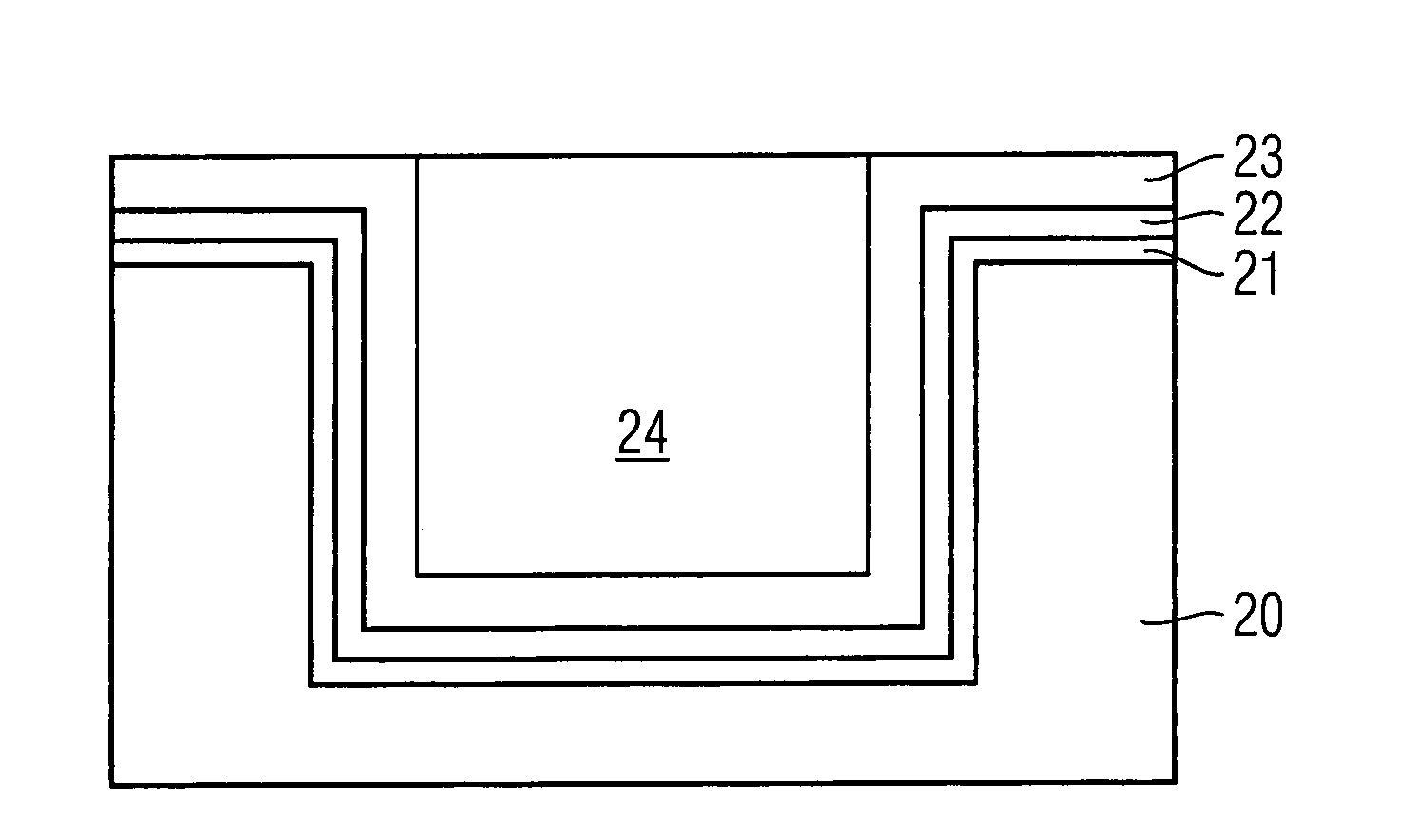
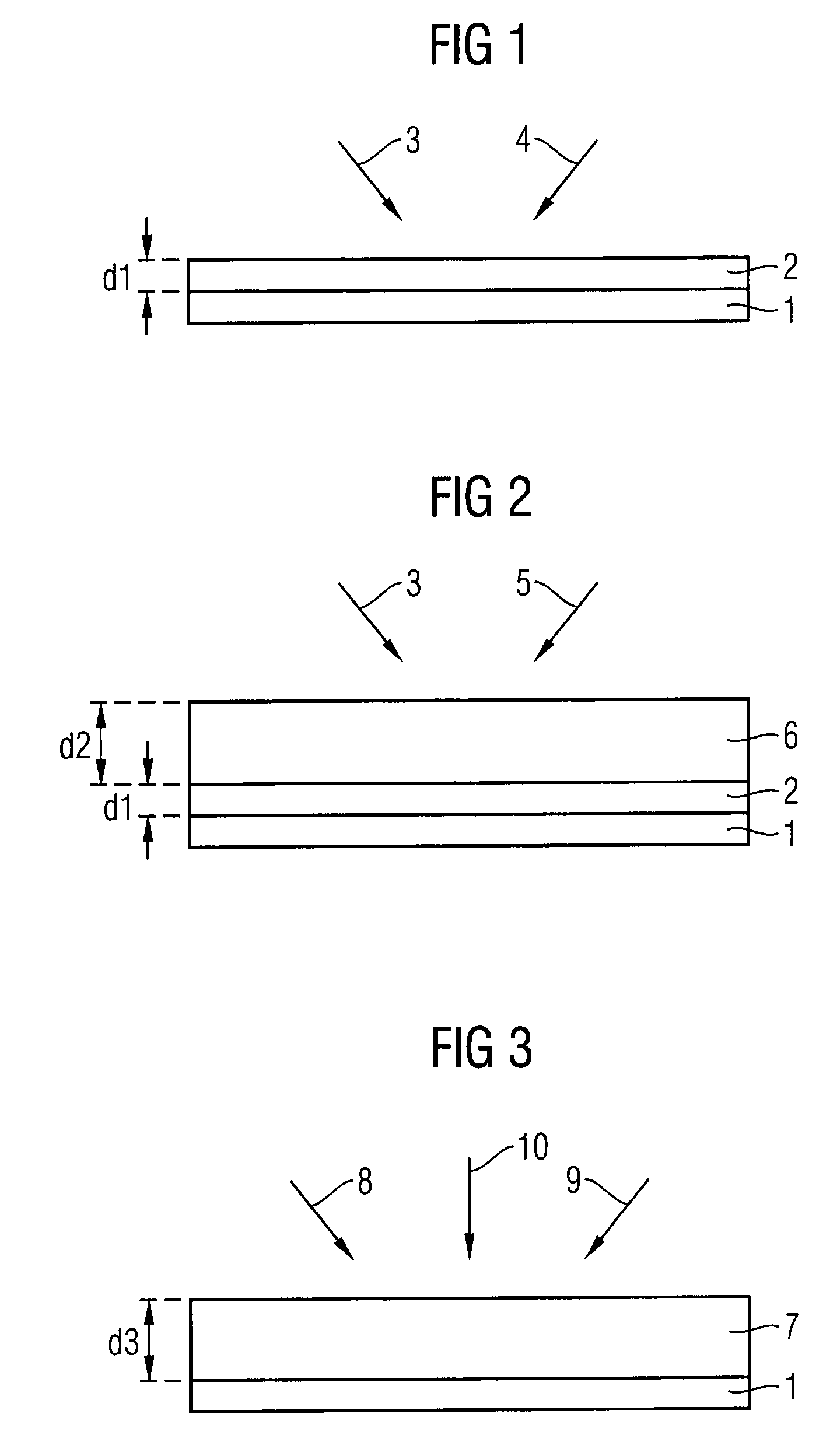
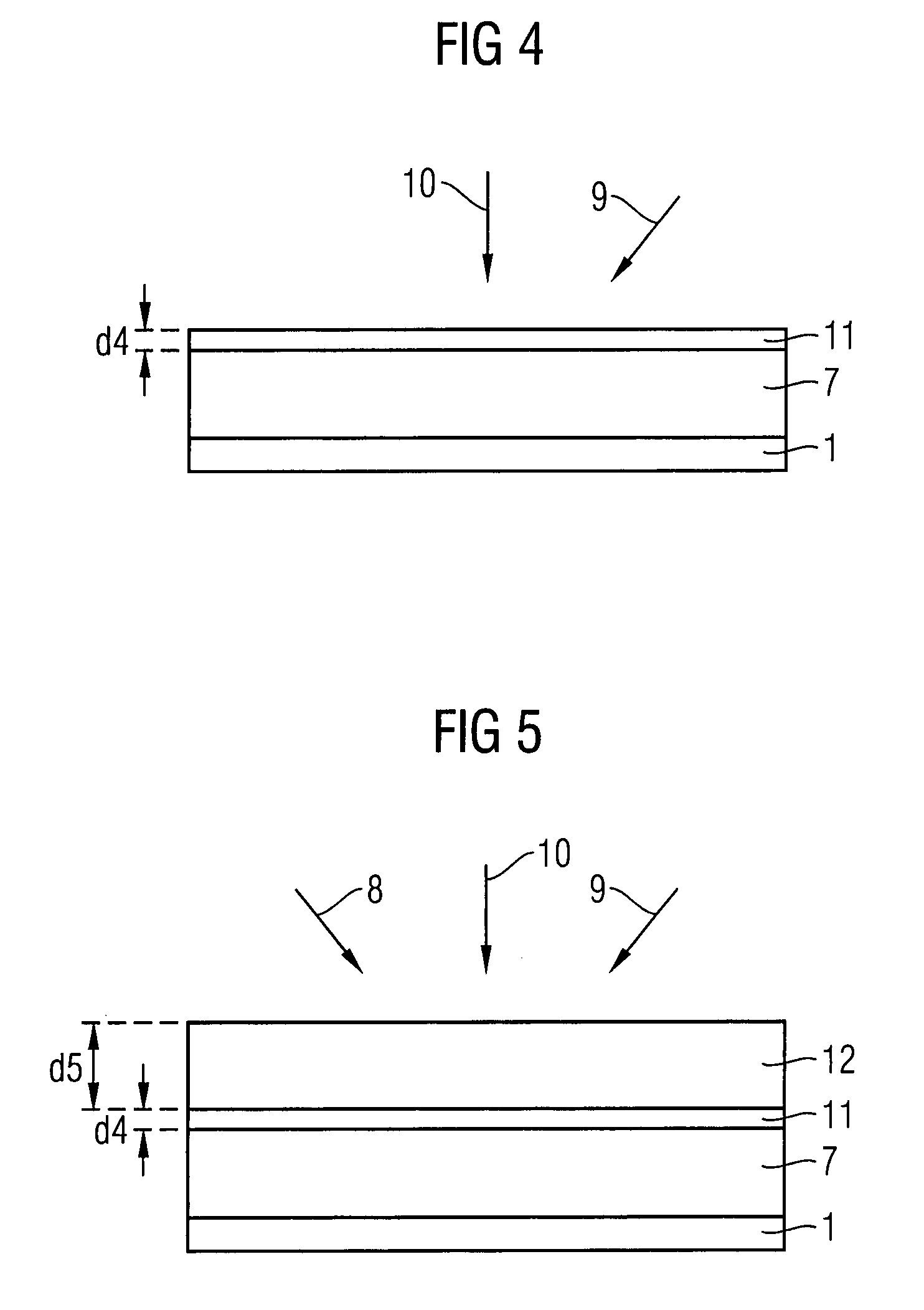
[0041]A first embodiment is illustrated along with the FIG. 1 and FIG. 2. Preferably a structured conductive layer is provided, later on called substrate 1, which may form a bottom electrode of a capacitor. The structured substrate 1 preferably comprises a titanium nitride based structure or of other specices of the group of carbon, tantalum nitride, tungsten, ruthenium and / or platinum.

[0042]In a first step of the first embodiment a dielectric layer 2 comprising zirconium oxide (ZrO) is deposited by an atomic layer deposition (ALD) method. The below description only mentions zirconium, but is not restricted to the use of zirconium. Hafnium can be used instead of or additional to zirconium, for instance.

[0043]A first pre-cursor 3 and a second pre-cursor 4 are introduced alternatingly into a reaction chamber, in which the substrate 1 is placed. The first pre-cursor is an organic compound to which a transition metal is coupled, by way of example tetrakis (ethyl methyl amido) zirconium ...


PUM

PropertyMeasurementUnit
thicknessaaaaaaaaaa
thicknessaaaaaaaaaa
temperaturesaaaaaaaaaa

Abstract

The present invention relates to a method for depositing a dielectric material comprising a transition metal compound. After providing a substrate, a first pre-cursor comprising a transition metal compound and a second pre-cursor predominantly comprising at least one of water vapour, ammonia and hydrazine are successively applied on the substrate for forming a first layer of transition metal containing material. In a next step the first pre-cursor and a third pre-cursor comprising at least one of ozone and oxygen are successively applied on the first layer for forming a second layer of the transition metal containing material.

Description

BACKGROUND OF THE INVENTION[0001]1. Field of the Invention[0002]The present invention relates to a deposition method for a transition-metal-containing dielectric.[0003]2. Description of the Related Art[0004]Although in principle applicable to arbitrary integrated semiconductor structures, the following invention and the underlying problems will be explained with respect to integrated DRAM memory circuits in silicon technology.[0005]Memory cells of a DRAM device each comprise a capacitor for storing information encoded as electric charge retained in the capacitor. A reliable operation of the memory cells demands for a minimal capacitance of the capacitors and a sufficiently long retention time of the charge in the capacitors.[0006]There is a major interest to further reduce the lateral dimensions of structures of a DRAM, at present 45 nm are envisaged. Therefore, it becomes necessary to compensate the shrinking lateral dimensions of the capacitors by increasing the k-value of the die...

Claims


Application Information

Patent Timeline
Patent Type & Authority Patents(United States)
IPC IPC(8): H01L21/20
CPCH01G4/10H01G4/33H01L21/3141H01L21/31641H01L21/31645H01L28/65H01L27/10852H01L21/02189H01L21/02181H10B12/033
Inventor KUDELKA, STEPHANOBERBECK, LARSSCHROEDER, UWEBOESCKE, TIMHEITMANN, JOHANNESSAENGER, ANNETTESCHUMANN, JOERGERBEN, ELKE
Owner POLARIS INNOVATIONS LTD
Why Eureka
Try Eureka