
Germanium doped n-type aluminum nitride epitaxial layers

a technology of aluminum nitride and nitride, which is applied in the direction of natural mineral layered products, polycrystalline material growth, crystal growth process, etc., can solve the problems of not being able to be used under any circumstances, obtaining blue light from semiconductors, and not being the only attractive produ

Inactive Publication Date: 2010-03-23
NORTH CAROLINA STATE UNIV +1
View PDF6 Cites 12 Cited by
  • Summary
  • Abstract
  • Description
  • Claims
  • Application Information

AI Technical Summary

Benefits of technology

[0014]Therefore, it is an object of the present invention to provide a method for successfully doping aluminum nitride with an n-type dopant that will produce effective n-type epitaxial layers.

Problems solved by technology

Many semiconductor materials have bandgaps that are generally smaller than this threshold, and thus cannot be used under any circumstance to produce blue light.
In turn, because blue is one of the three primary colors (along with red and green), the difficulty in obtaining blue light from semiconductor LEDs translates into an accompanying difficulty of producing full color LED displays or LED white light sources, each of which require some contribution of blue light.
Blue light emitting diodes (including lasers and ultraviolet diodes and lasers), are not, however, the only attractive product that can be formed by wide bandgap materials.
Aluminum nitride is a difficult material to work with.
The Group III nitrides are difficult to form into coherent bulk single crystals appropriate for substrates for semiconductor devices.
Thus, the requirement that other materials (such as sapphire) serve as substrates for such devices has to some extent limited their development.
Silicon has been demonstrated to work as an n-type dopant for gallium nitride but has not performed appropriately as an n-type dopant for aluminum nitride in attempts to date.
Doping of aluminum nitride has been particularly difficult to accomplish using the metal organic chemical vapor deposition technique (“MOCVD” or just “CVD”).
As a result, it appears that CVD techniques consistently tend to leave some amount of hydrogen (H2) in epitaxially grown films, and that the resulting hydrogen in the crystalline layer may interfere with the n-type doping in aluminum nitride.
Such scavenging is more likely to occur in a CVD system and thus interfere with the overall doping process.

Method used


Image

  • Germanium doped n-type aluminum nitride epitaxial layers
  • Germanium doped n-type aluminum nitride epitaxial layers

Examples


Embodiment Construction

[0021]The invention is an n-type epitaxial layer of aluminum nitride conductively doped with germanium. Because the invention provides such an n-type epitaxial layer of aluminum nitride, it can be incorporated with a substrate to form a device precursor, and in conjunction with both a substrate and another epitaxial layer, can comprise a rectifying diode.

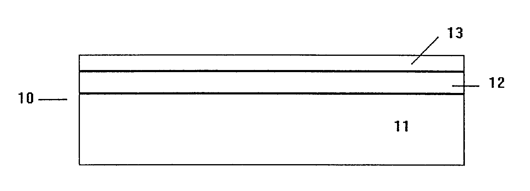
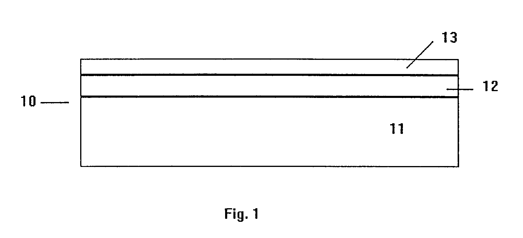
[0022]FIG. 1 illustrates such a rectifying diode broadly designated at 10 in which the substrate is designated at 11, the n-type aluminum nitride epitaxial layer according to the invention is indicated at 12, and a p-type layer of an appropriate semiconductor material is illustrated at 13.

[0023]A preferred material for the substrate 11 comprises silicon carbide which is most preferably selected from the 4H and 6H polytypes of silicon carbide because they currently offer the best crystal lattice match with aluminum nitride, and thus with the aluminum nitride layer 12. Presently, the 6H polytype of silicon carbide is more widely avail...


PUM

PropertyMeasurementUnit
Temperatureaaaaaaaaaa
Electrical conductoraaaaaaaaaa
Carrier concentrationaaaaaaaaaa

Abstract

A method of preparing an n-type epitaxial layer of aluminum nitride conductively doped with germanium comprises directing a molecular beam of aluminum atoms onto the growth surface of a substrate that provides an acceptable lattice match for aluminum nitride; directing a molecular beam of activated nitrogen to the growth surface of the substrate; and directing a molecular beam of germanium to the growth surface of the substrate; while maintaining the growth surface of the substrate at a temperature high enough to provide the surface mobility and sticking coefficient required for epitaxial growth, but lower than the temperature at which the surface would decompose or the epitaxial layer disassociate back into atomic or molecular species.

Description

[0001]This invention was made with Government support under Grant Nos. N00014-92-J-1720 and N00014-92-J-1477 awarded by the Office of Naval Research. The Government has certain rights in the invention.FIELD OF THE INVENTION[0002]The present invention relates to wide bandgap semiconductor materials and devices formed therefrom, and in particular relates to a method of forming an n-type aluminum nitride epitaxial layer doped with germanium and resulting device structures.BACKGROUND OF THE INVENTION[0003]Aluminum nitride (AlN) has been recognized for many years as a semiconductor material with a sufficiently wide bandgap to attract attention as a suitable material for electronic devices, including photonic (“optoelectronic”) devices such as light emitting diodes (LEDs). As used herein, the term light emitting diode refers to a semiconductor device which emits visible light (i.e. the portion of the electromagnetic spectrum visible to the human eye) when a potential difference is applied...

Claims


Application Information

Patent Timeline
IPC IPC(8): B32B18/00
CPCC30B23/02C30B29/403C30B29/406H01L21/02378H01L21/02433H01L21/02458H01L21/0254H01L21/02576H01L21/02631H01L29/2003H01L29/207H01L29/861H01L33/325
Inventor DAVIS, ROBERT F.WANG, CHENG
Owner NORTH CAROLINA STATE UNIV
Learn More