Internal antennae for plasma processing with metal plasma

a technology of metal plasma and plasma processing, applied in vacuum evaporation coatings, electrolysis components, coatings, etc., can solve the problems of complicated coil construction, low etch rate, and low etch uniformity, so as to reduce reduce the etch rate. , the effect of reducing the level of metal deposition

Inactive Publication Date: 2010-04-06
TOKYO ELECTRON LTD
View PDF18 Cites 13 Cited by
  • Summary
  • Abstract
  • Description
  • Claims
  • Application Information

AI Technical Summary

Benefits of technology

[0010]A further object of the invention is to combine the advantages and best features of the different approaches of the prior art that have not previously been available in a single apparatus, and to do so effectively and efficiently.
[0012]According to certain embodiments of the invention, a plasma source is provided having one or more of the following features: An internal coil shielded by a plasma shield where the coil and the shield are dimensioned to prevent the ignition of parasitic discharges around the RF coil. An internal coil shielded by a plasma shield where the plasma shield is designed to withstand high temperatures and to absorb most of the plasma heat load, and thereby eliminate the need to actively cool the RF coil. An internal coil behind which a backplate is provided that is RF and thermally grounded, wherein the backplate may be part of the chamber wall, and alternatively and preferably, is a separate removable component. An internal coil and backplate where the coil cross section is such that it reduces metal deposition on the backplate behind the coil. An internal coil where the shape of the RF coil is preserved by stiffeners mounted on the side facing the backplate. Coil stiffeners supporting a coil and including several radial stiffening members made of dielectric material that may be attached to the coil, preferably out of contact with the backplate. Coil stiffeners profiled, on the side facing the plasma, to prevent the formation of a conducting path of deposited material from one turn of the coil to the another. A coil and backplate assembly in which the backplate has grooves machined at locations corresponding to coil stiffening members, to preserve the design spacing of the backplate, preferably of 2 mm or less, from the coil. A coil and plasma shield wherein the shield is configured to absorb most of the plasma heat load and allow a non-negligible fraction of metal flux to deposit on the coil, which simplifies the profile of the shield and increases its RF transparency. Such a shield having several the radial slots for RF transmission. A vacuum seal for the coil RF feed. A coil and backplate assembly in which the center of the coil is thermally and electrically grounded to the backplate. A coil and backplate assembly having an RF feed connected to the outer part of the coil and vacuum seals against the backplate with a two-part sealing assembly.
[0013]There are several advantages of the features of the invention that accomplish the objectives of the invention and improve upon the prior art. The backplate can sustain a substantially larger amount of metal deposition than the dielectric window in the external coil configuration. Coil stiffeners keep the coil from sagging and coming into contact with the plasma shield. The backplate supports most of the atmospheric pressure against the vacuum. The advantages of this invention over other iPVD sources include a less restrictive requirement on metal flux shielding. The shield shields the coil from the plasma heat load. Some metal is allowed to pass through the shield and deposit on the coil, allowing a thinner shield with less complicated slots, and good RF transparency. The coil which need not be actively cooled, is not sputtered, and is thus not consumable, but may be cleaned from metal deposition from time to time. Since the coil is enclosed in a small conductive space, its inductance is about 50% less than in typical iPVD sources, resulting in reduced coil voltage, which can be exploited in two ways: 1) by simplifying some of the constraints on the design and construction of the tuning network and RF connectors, or 2) by at least partially trading off the reduced coil voltage for a reduced coil current, for example, by increasing the number of coil turns and thereby reducing the current through the coil. Such a source coil has a much lower profile than a three-dimensional OP coil.
[0015]Depending on the application, some of the features may be more or less important. In exclusively low-pressure applications, the requirements on the spacing of the backplate from the coil can be larger than 2 mm. Also, if the plasma heat load or sputtering is not excessive, as for example for operations in the range of several hundred watts, the plasma shield may be omitted. At the opposite extreme, for very high density plasmas, active cooling of the coil and plasma shield may be necessary. Also, depending on applications, the level of metal deposition on the ground plane and stiffeners may be unacceptable. In that case, the coil cross section may be changed from a rectangular shape to a chevron shape, so that the coil conductors themselves block line of sight paths through the coil. While more complex, this configuration will substantially reduce the level of metal deposition behind the coil
[0016]In etch applications, the present invention results in a uniform, high etch rate at a reduced voltage. Other applications of the invention allow a pre-clean step to be performed in situ in an IPVD module.

Problems solved by technology

Often, such a plasma also dramatically reduces the etch uniformity.
In addition, due to the large plasma thermal load, the coil needs to be water-cooled, complicating coil construction.
This approach removes some of the problems of the internal coil design, but suffers from the drawbacks of deposition shield complexity.
These goals are not easily accomplished, as one is usually achieved at the expense of the other.
Both types of shields introduce transmission losses and result in reduced efficiency of the RF source.
This in turn leads to increased complexity of other parts of the RF circuit, such as the tuning network and RF connectors from the coil to the tuning network.

Method used


Image

  • Internal antennae for plasma processing with metal plasma
  • Internal antennae for plasma processing with metal plasma
  • Internal antennae for plasma processing with metal plasma

Examples


Embodiment Construction

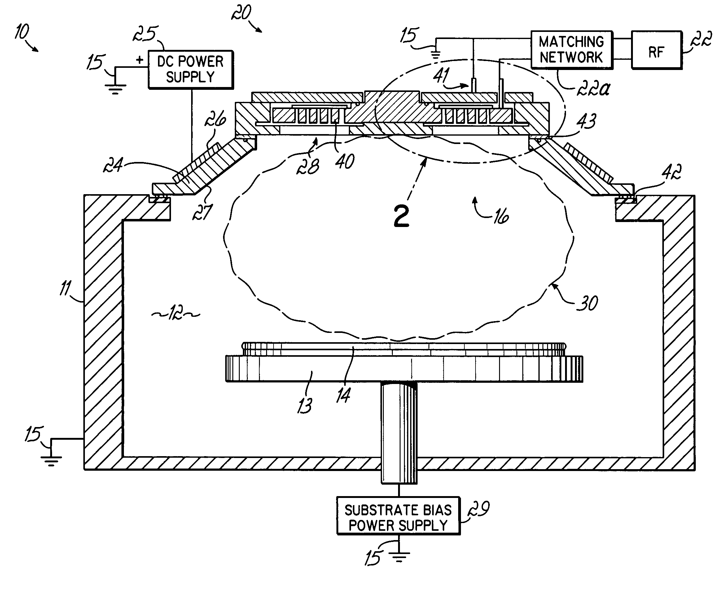
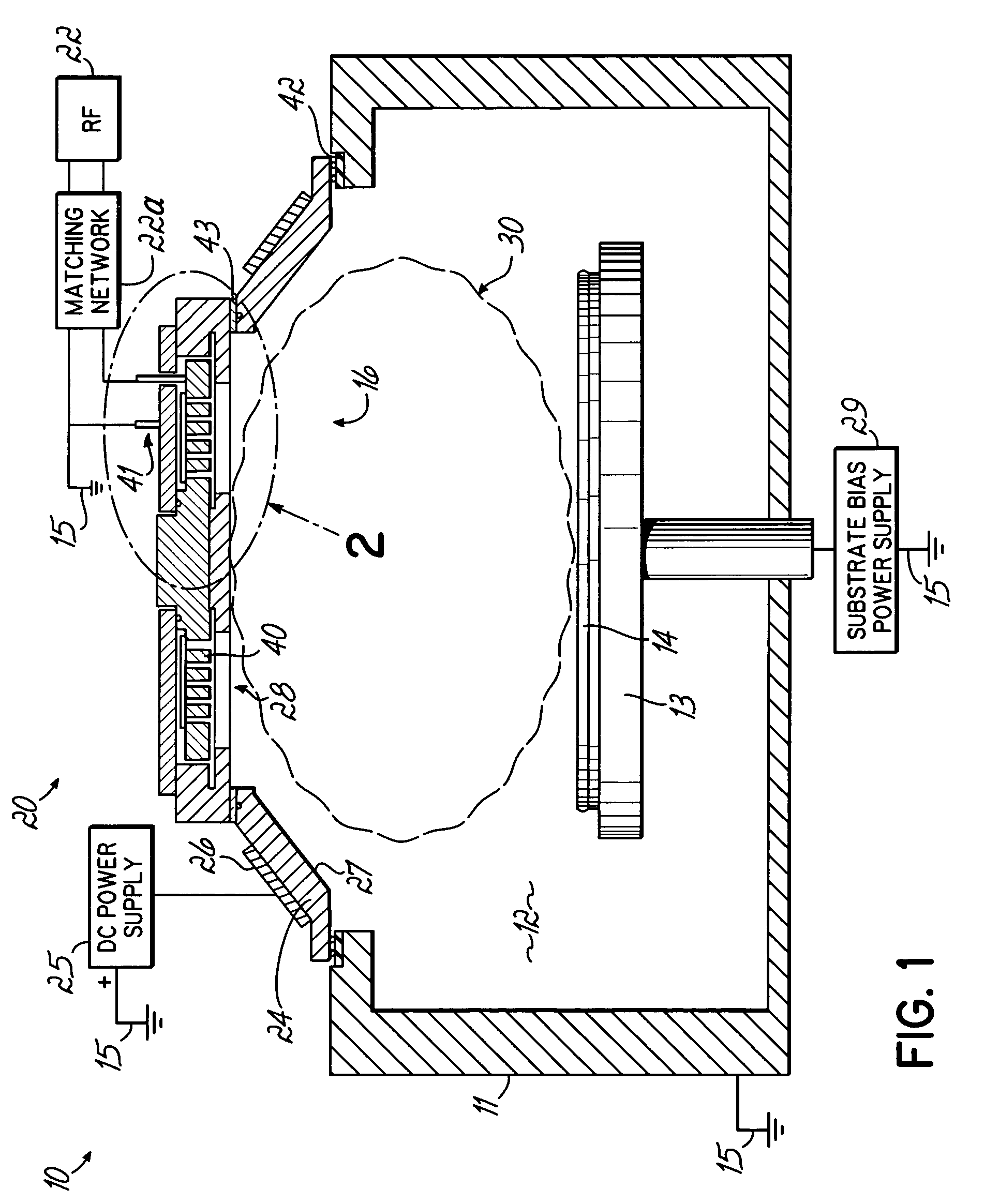
[0027]FIG. 1 illustrates an iPVD apparatus 10 of a type described in U.S. Pat. Nos. 6,287,435 and 6,719,886. The apparatus 10 includes a vacuum processing chamber 12 enclosed by a grounded metal chamber wall 11. An upwardly facing wafer support 13 supports a semiconductor wafer 14 in the chamber 12 for processing. In a circular opening 16 in the upper surface of the chamber wall 11, is a coating material source that includes a frusto-conical sputtering target 24 formed of the material, typically a metal, with which surfaces on the wafer 14 are to be coated. A permanent magnet pack 26 lies behind the target 24 and provides a plasma confining static magnetic field over the sputtering surface 27 of the target 24. A DC power source 25 is connected between the target 24 and a system ground 15 to apply a negative DC sputtering potential to the target 24. An RF bias power supply 29 is connected between the substrate support 13 and the system ground 15.

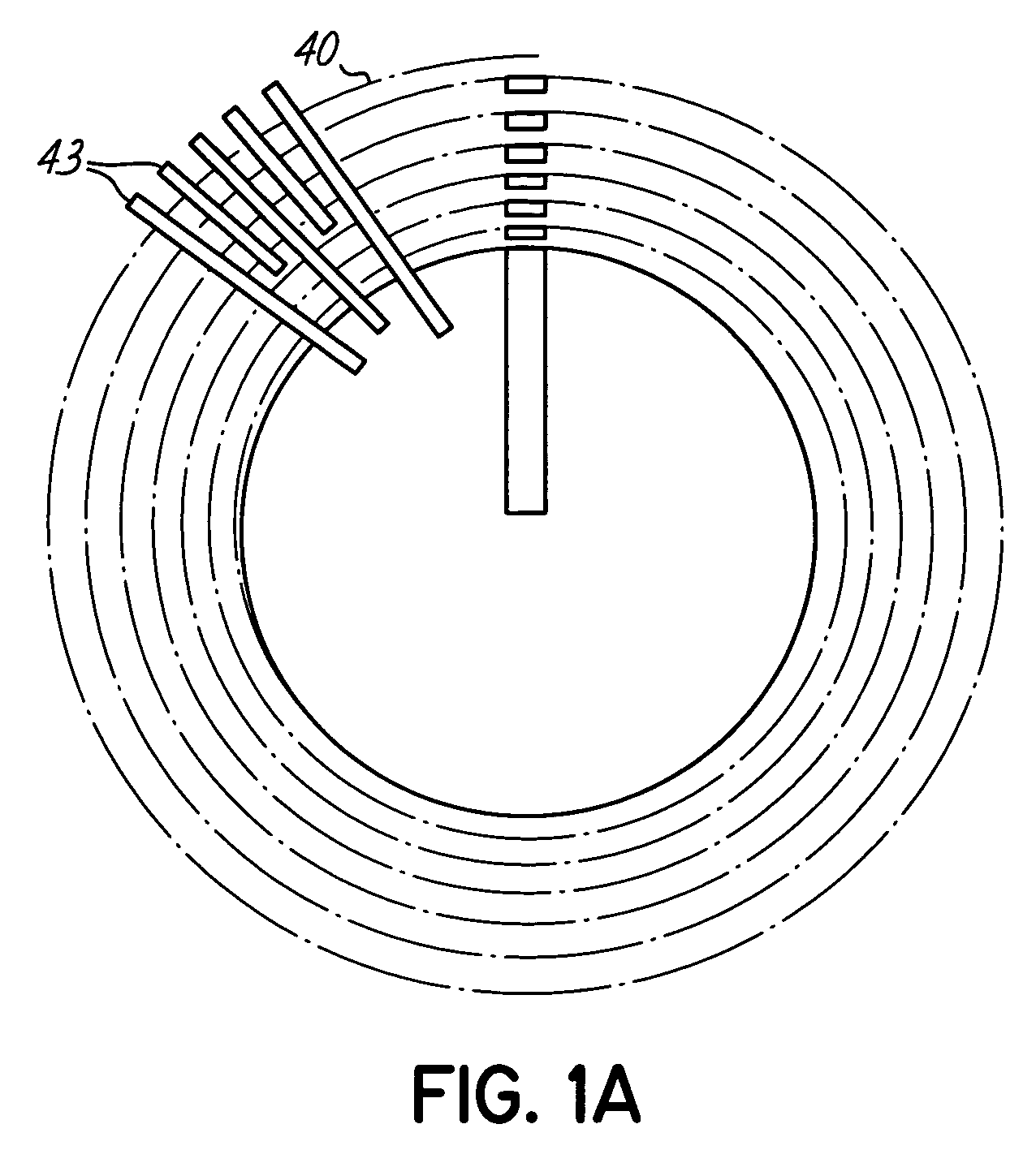
[0028]In an opening 28 at the center o...


PUM

PropertyMeasurementUnit
bias voltageaaaaaaaaaa
areaaaaaaaaaaa
frequenciesaaaaaaaaaa

Abstract

A plasma processing system and method provide an internal coil in a vacuum chamber for maintaining a high density plasma therein in a manner that may have a less restrictive requirement on metal flux shielding than when the shield protects a dielectric window. The shield also shields the coil from plasma heat load. The coil need not be actively cooled. Some metal is allowed to pass through the shield and deposit on the coil. This leads to a thinner shield with less complicated slots than for shields in external coil configurations. Good RF transparency of the shield is a result of the much simpler shield shape. The coil is not sputtered and is thus not consumable. The coil is enclosed in a small conductive space, reducing its inductance, resulting in reduced coil current and voltage, in turn simplifying the design and construction of the tuning network and RF connectors. Stiffeners support the coil and are profiled to avoid formation of conductive paths forming from metal deposits.

Description

[0001]This invention relates to the energizing of high density RF plasmas within the vacuum processing chambers of a plasma processing apparatus, and more particularly, to the use of antennae for coupling of RF energy into plasmas containing metal vapor or metal ions.BACKGROUND OF THE INVENTION[0002]In the deposition of metal onto semiconductor wafers in semiconductor manufacturing, plasma sources are used, in addition to a primary sputtering plasma source, to improve the performance of the processing tool. For instance, in ionized physical vapor deposition (iPVD) of metal onto a wafer, a supplemental plasma source is often used to increase plasma density to produce an increased fractional ionization of the metal atoms being deposited. This, combined with RF bias on the substrate wafer leads to improved coverage of the features on the wafer surface, and reduces the closing-off of the necks of such features. Likewise during a soft-etch stage that accompanies many iPVD and other proce...

Claims


Application Information

Patent Timeline
Patent Type & Authority Patents(United States)
IPC IPC(8): C25B9/00C23C14/00C23C16/00C25B11/00C25B13/00H01J37/32
CPCH01J37/32477H01J37/321
Inventor VUKOVIC, MIRKO
Owner TOKYO ELECTRON LTD
Why Eureka
Try Eureka