Exposure apparatus, exposure method, device manufacturing method, and system

a technology of exposure apparatus and exposure method, which is applied in the direction of focusing aids, printing, instruments, etc., can solve the problems of inability to ignore the oscillation of laser beams from laser light sources, and achieve the effects of easy calibration of each spectral monitor, good accuracy and good precision

Active Publication Date: 2010-04-20
NIKON CORP
View PDF14 Cites 31 Cited by
  • Summary
  • Abstract
  • Description
  • Claims
  • Application Information

AI Technical Summary

Benefits of technology

[0011]According to the apparatus, the spectral control unit performs a spectral width control of the laser beam so as to suppress the size error, based on the pattern size error-spectral characteristic information, which shows the relation between the size error of the pattern formed on the object and the spectral characteristic of the laser beam emitted from the laser unit, and information related to the pattern that is to be used.
[0015]According to this method, information of the total exposure amount of the laser beam emitted from the laser light source is obtained, and based on the information of the total exposure amount that has been obtained, the spectral width correction value is decided. In this case, for example, the spectral width correction value can be decided so that the size error of the pattern does not occur. Accordingly, by performing exposure of the object by adjusting the spectral width of the laser beam output from the laser light source to the spectral width that has been computed, the pattern can be formed without a size error on the object.
[0016]Further, in a lithography process, by performing exposure of a sensitive object using one of the first and second exposure methods of the present invention, it becomes possible to form a device pattern on the sensitive object with good precision. Accordingly, from a fourth aspect of the present invention, it can also be said that the present invention is a device manufacturing method that uses one of the first and second exposure methods of the present invention.
[0018]According to the system, by performing calibration of the spectroscope using the reference light source and performing spectral width measurement of the laser beam output from the plurality of laser units, it becomes possible to measure the spectral width of the laser beam output from each laser unit with good precision. Further, in the case each laser unit has a spectral monitor, by performing simultaneous measurement of the spectral width of the laser beam by using the calibrated spectroscope and each spectral monitor, it becomes possible to calibrate each spectral monitor easily and with good accuracy.

Problems solved by technology

As the cause of linewidth error after the OPC, various causes that change spectral characteristics of the laser beam oscillated from the laser light source are also becoming a cause that cannot be ignored.

Method used


Image

  • Exposure apparatus, exposure method, device manufacturing method, and system
  • Exposure apparatus, exposure method, device manufacturing method, and system
  • Exposure apparatus, exposure method, device manufacturing method, and system

Examples


first embodiment

A First Embodiment

[0027]A first embodiment of the present invention is described below, referring to FIGS. 1 to 7.

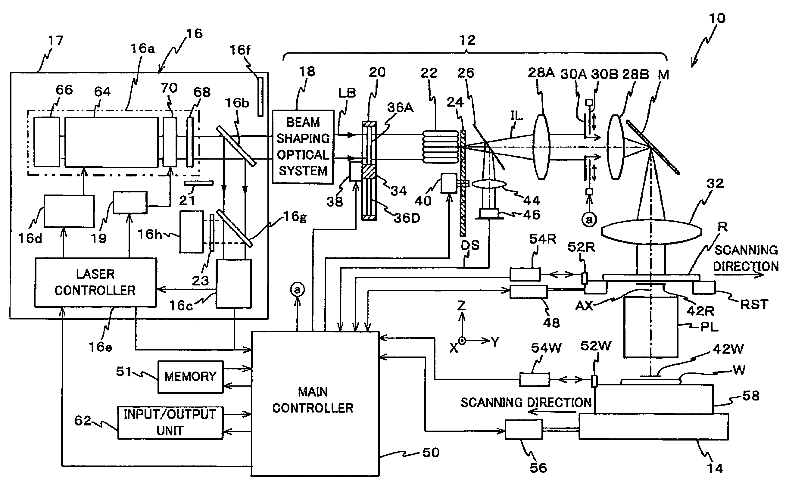
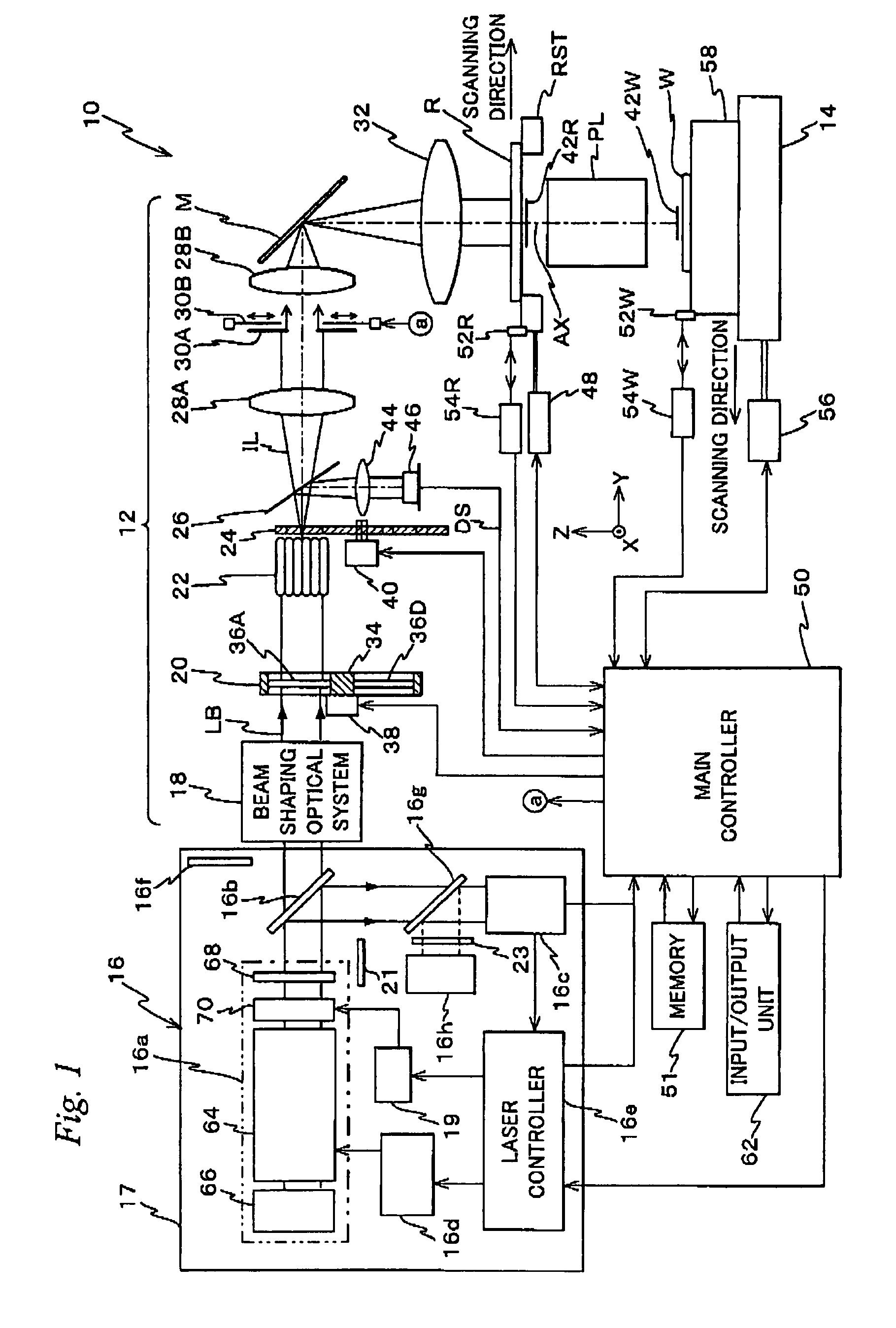
[0028]FIG. 1 is an entire view of an arrangement of an exposure apparatus 10 related to the first embodiment. Exposure apparatus 10 is a scanning exposure apparatus based on a step-and-scan method that uses a laser unit for an exposure light source.

[0029]Exposure apparatus 10 is equipped with an illumination system that includes a laser unit 16 and an illumination optical system 12, a reticle stage RST that moves in a predetermined scanning direction (in this case, a Y-axis direction, which is the lateral direction within the page surface of FIG. 1) holding a reticle R illuminated by the illumination system, a projection optical system PL that projects an image of a pattern of reticle R on a wafer W, an XY stage that moves within a horizontal plane (an XY plane) holding wafer W, a control system for these components and the like.

[0030]As laser unit 16, for instance, a Kr...

second embodiment

A Second Embodiment

[0130]Next, a second embodiment of the present invention will be described below, referring to FIG. 8. The system in the second embodiment is equipped with a plurality of laser units, which serve as a light source for each of a plurality of exposure apparatus. However, in the description below, from the viewpoint of avoiding complication, details on only two laser units 16A and 16B will be described. Further, the same reference numerals will be used for the sections that are the same or similar to the first embodiment described above, and the description thereabout will be omitted.

[0131]Laser units 16A and 16B shown in FIG. 8 are each configured similar to laser unit 16 described earlier, except for the point that reference light source 16h, half mirror 16g, shutters 21 and 23 are not arranged. On the optical path of a laser beam LB1 emitted from laser resonator 16a of laser unit 16A, a beam splitter 72 is arranged that has a transmittance of around 97%. On the op...


PUM


Abstract

An exposure apparatus is equipped with a laser unit that emits a laser beam, a memory that stores a first information which shows a first relation indicating a relation between a linewidth error of a pattern formed on a wafer and a spectral characteristic of the laser beam emitted from the laser unit, and a main controller that controls the spectral width of the laser beam via a laser controller, based on the first information and on information related to a reticle that is to be used. Main controller performs spectral width control of the laser beam so as to suppress linewidth error, based on the first information and on the information related to the reticle that is to be used.

Description

TECHNICAL FIELD[0001]The present invention relates to exposure apparatus, exposure methods, device manufacturing methods, and systems, and more particularly to an exposure apparatus that is equipped with a laser unit as an exposure light source, an exposure method performed with the exposure apparatus, a device manufacturing method using the exposure method, and a system that includes a plurality of laser units.BACKGROUND ART[0002]In recent years, in a sequentially moving type exposure apparatus such as a stepper or a scanning stepper (also called a scanner), a spectrum narrowed pulse oscillation excimer laser of a discharged pumped type is used as the light source. The pulse beam oscillated from the excimer laser passes the illumination optical system of the exposure apparatus main body and is irradiated on the photosensitive agent coated on the surface of the wafer mounted on the wafer stage exposing the photosensitive agent, and the wafer is exposed.[0003]As for the spectral widt...

Claims


Application Information

Patent Timeline
Patent Type & Authority Patents(United States)
IPC IPC(8): G03B27/42G03B27/52
CPCG03F7/7005G03F7/70458G03F7/70525G03F7/70558G03F7/70575G03F7/70625H01S2301/08H01S3/10069H01S3/1055H01S3/1394H01S3/225G03F7/70025
Inventor ARAI, MASAYOSHI
Owner NIKON CORP
Why Eureka
Try Eureka