Method of forming memory with floating gates including self-aligned metal nanodots using a coupling layer

a technology of metal nanodots and coupling layers, which is applied in the field of memory having charge-storing nanodots, can solve the problems that existing techniques are not satisfactory in providing nanodots with uniform size and alignmen

Active Publication Date: 2010-05-25
SANDISK TECH LLC
View PDF29 Cites 26 Cited by
  • Summary
  • Abstract
  • Description
  • Claims
  • Application Information

AI Technical Summary

Problems solved by technology

However, existing techniques have not been satisfactory in providing nanodots which have a uniform size and alignment, and which can be easily used with existing fabrication techniques.

Method used


Image

  • Method of forming memory with floating gates including self-aligned metal nanodots using a coupling layer
  • Method of forming memory with floating gates including self-aligned metal nanodots using a coupling layer
  • Method of forming memory with floating gates including self-aligned metal nanodots using a coupling layer

Examples


Embodiment Construction

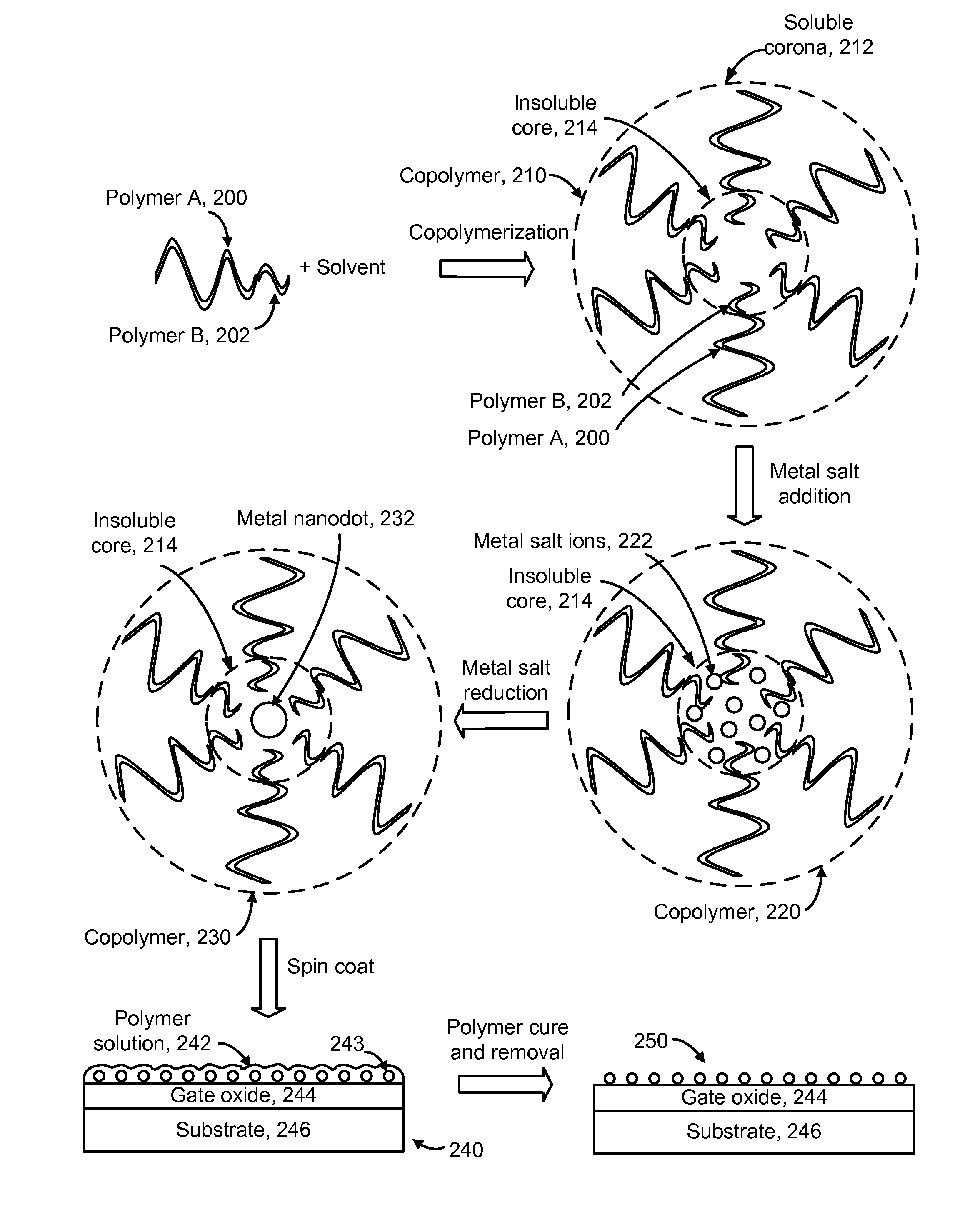
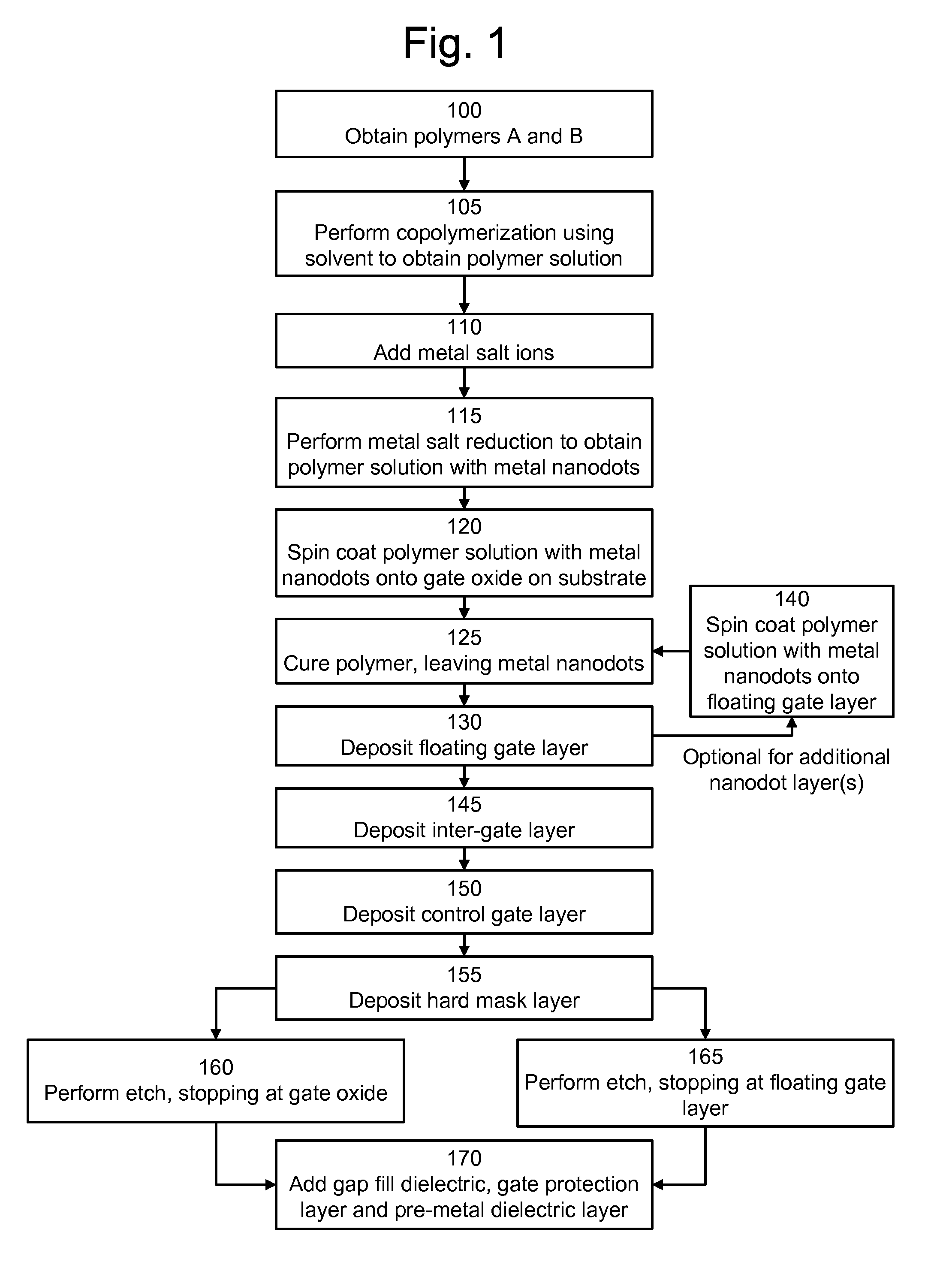
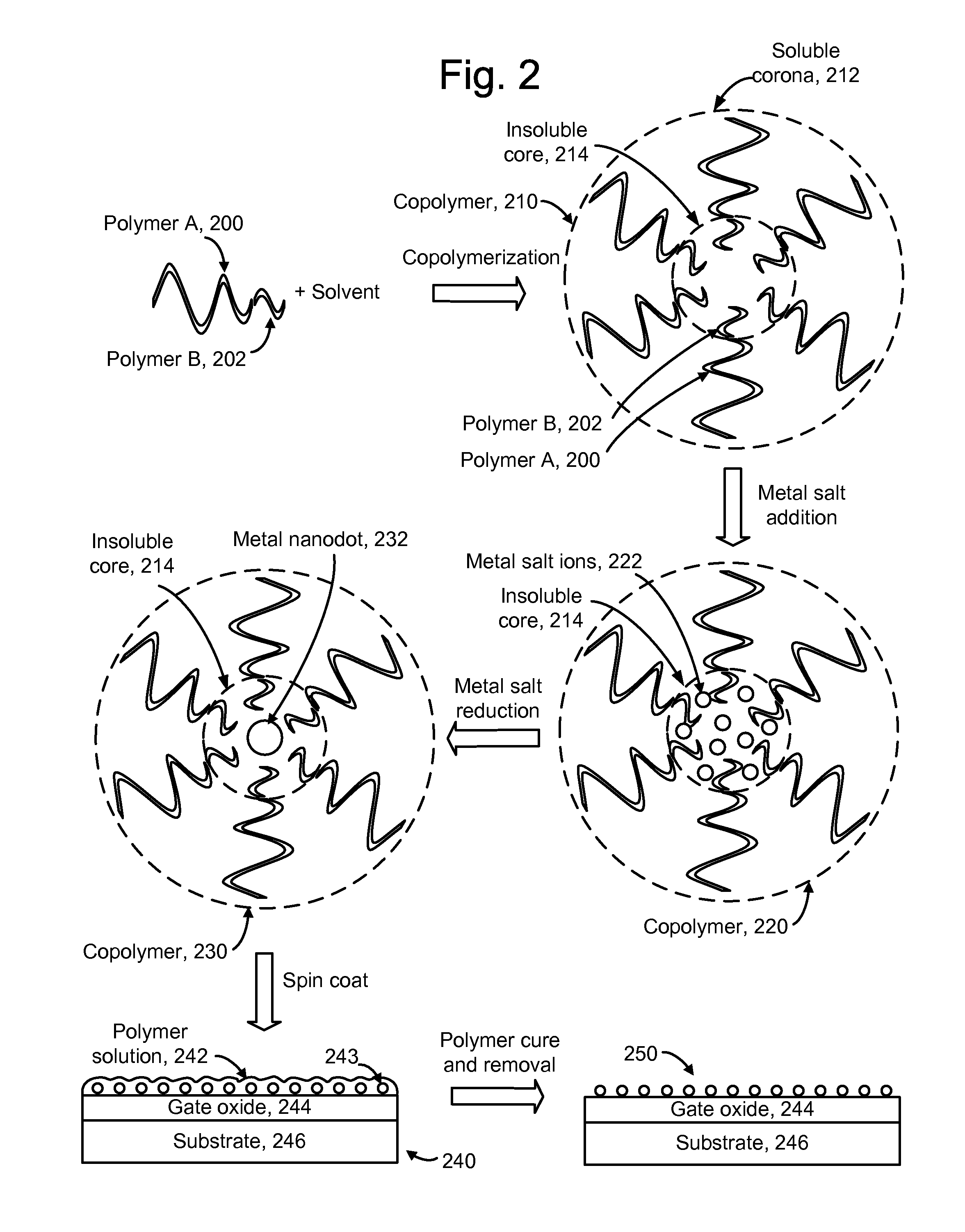
[0035]The present invention provides a method for fabricating memory having charge-storing, self-aligned metal nanodots by applying the nanodots to a substrate using a coupling layer.

[0036]In a storage element, nanodots can be used to store charge (e.g., electrons). The use of nanodots as charge-storing particles in memory such as non-volatile memory provides many advantages, including allowing reduced programming voltages, resulting in reduced power / current consumption in the memory device, and scaling to ever smaller dimensions in future generation memory devices. Further, nanodots are compatible with conventional fabrication techniques and materials.

[0037]During fabrication, a 2D array of nanodots is formed on a substrate with a uniform nanodot size and alignment. Vacuum deposition techniques such as sputtering and evaporation may not be adequate in controlling the alignment of the nanodots and may allow the nanodots to pile up on the edges of steps and / or trenches on the substra...


PUM


Abstract

Techniques are provided for fabricating memory with metal nanodots as charge-storing elements. In an example approach, a coupling layer such as an amino functional silane group is provided on a gate oxide layer on a substrate. The substrate is dip coated in a colloidal solution having metal nanodots, causing the nanodots to attach to sites in the coupling layer. The coupling layer is then dissolved such as by rinsing or nitrogen blow drying, leaving the nanodots on the gate oxide layer. The nanodots react with the coupling layer and become negatively charged and arranged in a uniform monolayer, repelling a deposition of an additional monolayer of nanodots. In a configuration using a control gate over a high-k dielectric floating gate which includes the nanodots, the control gates may be separated by etching while the floating gate dielectric extends uninterrupted since the nanodots are electrically isolated from one another.

Description

BACKGROUND OF THE INVENTION[0001]1. Field of the Invention[0002]The present invention relates to memory having charge-storing nanodots.[0003]2. Description of the Related Art[0004]Semiconductor memory has become increasingly popular for use in various electronic devices. For example, non-volatile semiconductor memory is used in cellular telephones, digital cameras, personal digital assistants, mobile computing devices, non-mobile computing devices and other devices. Electrically Erasable Programmable Read Only Memory (EEPROM) and flash memory are among the most popular non-volatile semiconductor memories. With flash memory, also a type of EEPROM, the contents of the whole memory array, or of a portion of the memory, can be erased in one step, in contrast to the traditional, full-featured EEPROM.[0005]Both the traditional EEPROM and the flash memory utilize a floating gate that is positioned above and insulated from a channel region in a semiconductor substrate. The floating gate is ...

Claims


Application Information

Patent Timeline
Patent Type & Authority Patents(United States)
IPC IPC(8): H01L21/336H01L21/30
CPCB82Y10/00H01L21/28273H01L29/42332H01L27/11521H01L29/42324H01L27/115Y10S977/81Y10S438/962Y10S977/943Y10S977/72H01L29/40114H10B69/00H10B41/30
Inventor PURAYATH, VINOD ROBERTMATAMIS, GEORGEORIMOTO, TAKASHIKAI, JAMESPHAM, TUAN D.
Owner SANDISK TECH LLC
Why Eureka
Try Eureka