Electron beam processing for mask repair

a technology of electron beam and mask, applied in the field of charged particle beam processing, can solve the problems of affecting the transmission of light through the substrate, reducing the size of the structure that can be produced, and requiring repair of defects, so as to reduce the light transmissivity, reduce the thickness of the substrate, and reduce the effect of light transmissivity

Inactive Publication Date: 2010-06-01
FEI CO
View PDF29 Cites 8 Cited by
  • Summary
  • Abstract
  • Description
  • Claims
  • Application Information

AI Technical Summary

Benefits of technology

[0008]The present invention entails directing an electron beam to a substrate having reduced light transmissivity, for example, from gallium atoms incidentally implanted by a focused ion beam used to remove material. In some embodiments, the electron beam is directed to the substrate, preferably in the presence of a gas, at a beam energy and dose such that the thickness of the substrate is not substantially decreased by the electron beam bombardment, yet the transmissivity of the substrate is substantially increased. By maintaining a thickness close to that of the original mask, the effect of the mask repair on the phase of the transmitted radiation is minimize. In other embodiments, the thickness of the substrate is decreased as the transparency is restored.

Problems solved by technology

The size of the structure that can be produced is limited by the wavelength of radiation used; shorter wavelengths can produce smaller structures.
Some photolithography masks used with such short wavelengths use reflective, rather than a transmissive, patterns on the masks because the substrates are not sufficiently transparent to such small wavelengths of radiation.
Most newly fabricated masks have some defects such as missing or excess pattern material and, before such masks can be used, the defects must be repaired.
Unfortunately, the ion beam also damages the mask surface and implants ions into the substrate, which adversely affects the transmission of light through the substrate.
Removing substrate material, however, changes the thickness of the substrate, which in turn changes the phase of the transmitted light.
The altered phase alters the aerial image, adversely affecting mask performance, particularly in a phase shift mask.
Also, there are limits to how much implanted gallium can be removed by a process that entails directing a gallium beam toward the surface.

Method used


Image

  • Electron beam processing for mask repair
  • Electron beam processing for mask repair
  • Electron beam processing for mask repair

Examples


Embodiment Construction

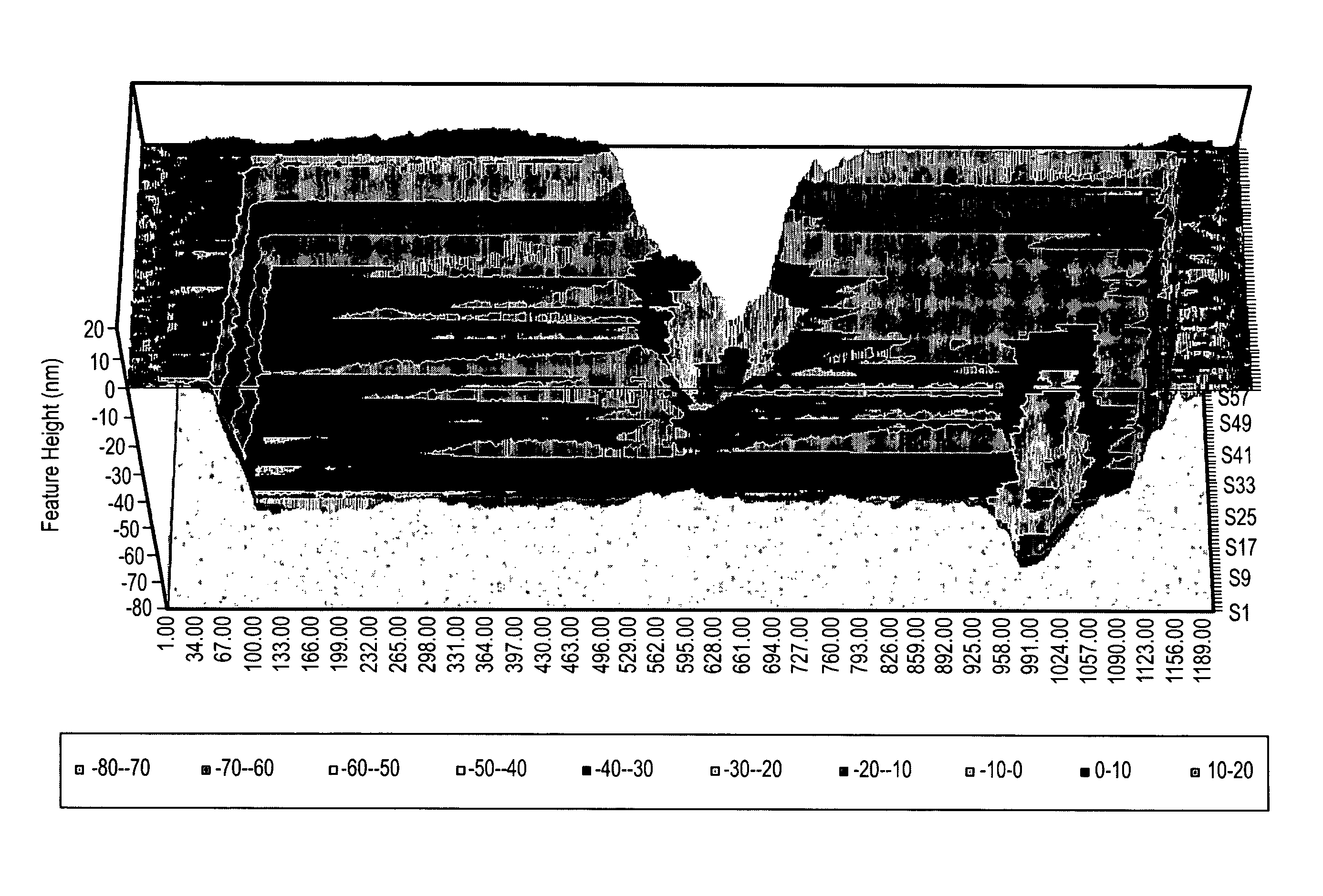
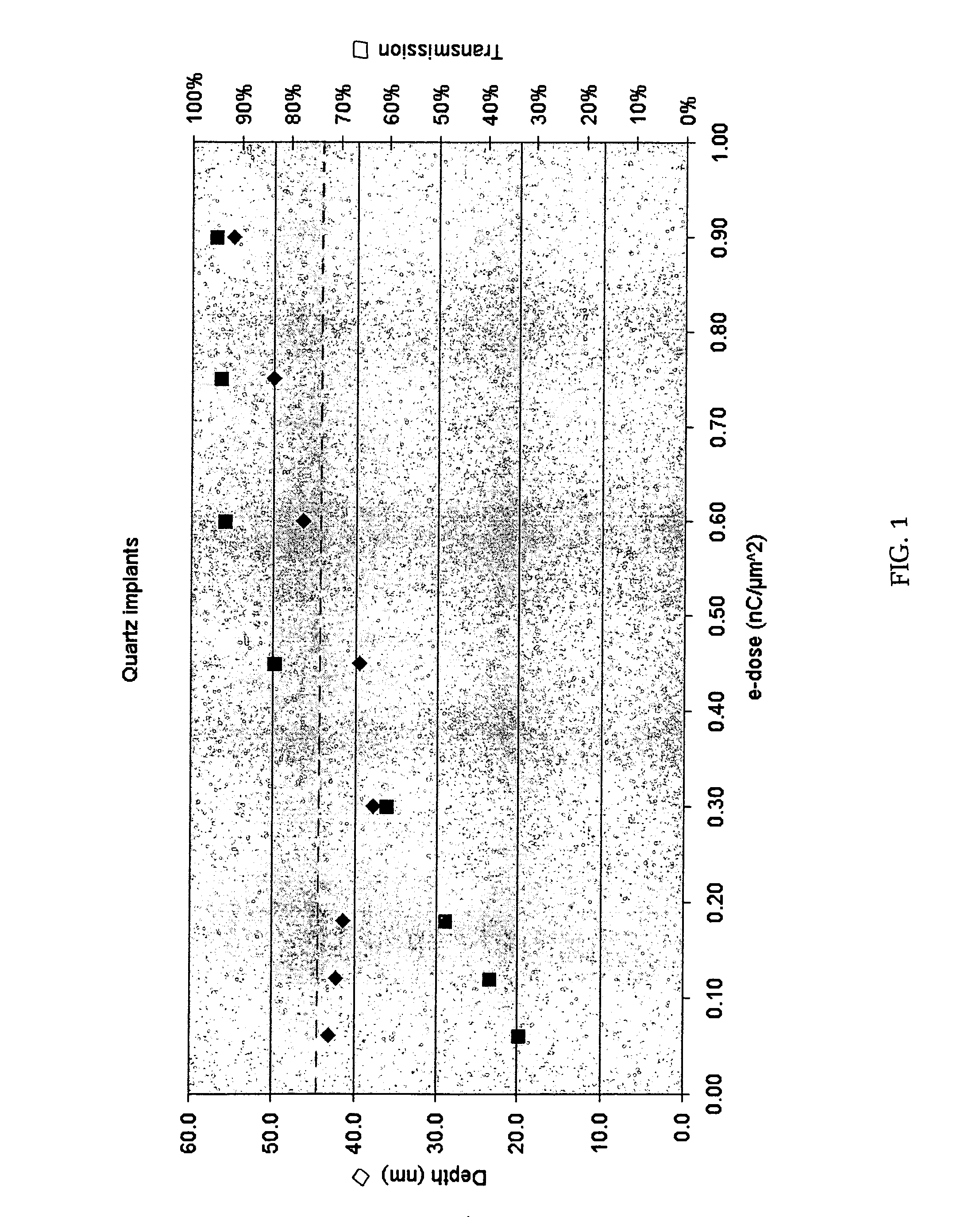
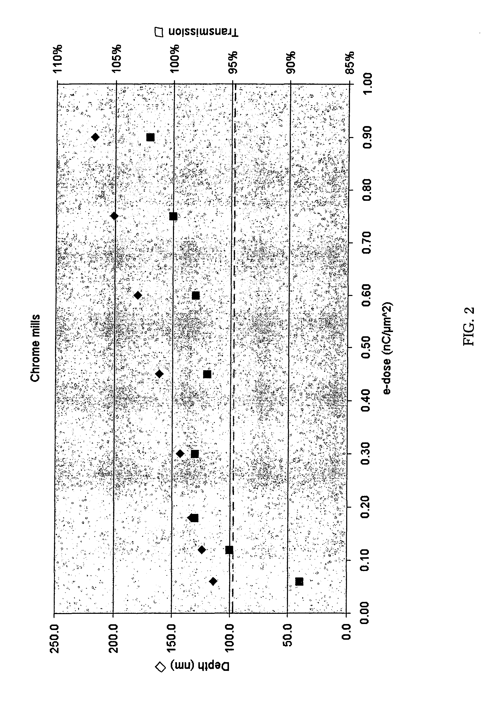
[0023]As described above, directing a beam of gallium ions towards the quartz surface reduces the transparency of the surface, thereby adversely affecting the performance of a quartz photolithography mask. Although this decrease in transparency can be intentionally used to make a portion of a mask relatively opaque, an incidental decrease in transparency can also be an undesirable side effect when a gallium ion beam is used to repair an area that is not intended to be opaque.

[0024]Applicants have found that the transparency of the repaired area can be restored by directing an electron beam in the presence of an etch-enhancing gas toward the repaired area. Applicants have found that the effect of this process varies with the concentration of implanted gallium.

[0025]When the implanted gallium is at a relatively high concentration, applicants have found that the transparency of the repaired area can be restored without a substantial change in the substrate thickness. In some cases, the...


PUM

PropertyMeasurementUnit
thicknessaaaaaaaaaa
thicknessaaaaaaaaaa
thicknessaaaaaaaaaa

Abstract

Transmissivity is restored to a gallium stained substrate by directing an electron beam to the substrate in the presence of an etching gas. For higher concentrations of implanted gallium, the transparency can be substantially restored without reducing the thickness of the substrate. For lower doses of implanted gallium, the transmission is restored to 100%, although the thickness of the substrate is reduced. The invention is suitable for use in the repair of photolithography masks.

Description

TECHNICAL FIELD OF THE INVENTION[0001]The present invention relates to charged particle beam processing to repair defects on lithography masks.BACKGROUND OF THE INVENTION[0002]Photolithography is a process that is used to create small structures, such as integrated circuits and micromachines. The photolithography process entails exposing a radiation-sensitive substance, called photoresist, to a pattern of light or other radiation. The pattern is typically created by passing the radiation through a mask, which is composed of a substrate with a pattern on its surface. The pattern blocks some of the radiation or changes its phase to create exposed and unexposed areas on the radiation-sensitive material. In a binary intensity mask, the pattern is made of a light absorbing material on an otherwise transparent substrate. In a phase shift mask, the pattern consists of material that shifts the phase of the light passing through it to create an interference pattern on the photoresist that pr...

Claims


Application Information

Patent Timeline
Patent Type & Authority Patents(United States)
IPC IPC(8): B01J19/08C03C15/00C23F1/00C23F1/02C23F3/00G03FG03F1/00G03F9/00G21K5/10H01L21/027
CPCG03F1/74H01J2237/31744
Inventor STEWART, DIANE K.CASEY, JR., J. DAVIDCASEY, LEGAL REPRESENTATIVE, JOAN WILLIAMSBEATY, JOHNMUSIL, CHRISTIAN R.BERGER, STEVENSIJBRANDIJ, SYBREN J.
Owner FEI CO
Why Eureka
Try Eureka