Integrated circuit

a technology of integrated circuits and components, applied in the direction of instruments, discharge tube main electrodes, code conversion, etc., can solve the problems of increasing leakage current, large number of elements, and insufficient conventional scaling factor,

Inactive Publication Date: 2010-06-08
YOKOGAWA ELECTRIC CORP
View PDF19 Cites 0 Cited by
  • Summary
  • Abstract
  • Description
  • Claims
  • Application Information

AI Technical Summary

Benefits of technology

[0015]A very high-speed light-receiving integrated circuit for optical communication is constructed by utilizing a very high-speed optical response characteristic of electron emission of the vacuum element, and a sensor such as a magnetic / electric field sensor is constructed by utilizing a quantum effect of ballistically traveling electrons.

Problems solved by technology

That is, an extremely large number of elements are required.
However, as the progress of the X-ray exposure technique and the electron beam exposure technique has enabled ultrafine processing of 0.065 μm or less, the influence of a tunnel effect, which is a physical phenomenon, causes increase in leakage current, injection of hot electrons, avalanche breakdown and the like occur in a MOS oxide film, which is a conventionally used insulating material.
Therefore, the conventional scaling factor cannot suffice and a problem arises that the operation becomes unstable in an LSI.
Although a one-electron transistor or the like is proposed as an ultimate element, it requires a cryogenic environment and its one-electron quantum effect makes the operation unstable under the law of quantum-mechanical establishment.
However, there is a problem that it is extremely difficult to generate quantum interference in a solid substance at a room temperature because of the influence of various scattering effects (impurity scattering, phonon scattering and the like).

Method used


Image

  • Integrated circuit
  • Integrated circuit
  • Integrated circuit

Examples


Embodiment Construction

[0030]An embodiment of an integrated circuit according to this invention will now be described with reference to the drawings. Superconducting AD and superconducting ALU (arithmetic logic unit) have already proven that a logical circuit that may be realized by tens of thousands to millions of semiconductor transistors can be realized by several to tens or hundreds of quantum effect-applied elements.

[0031]In this invention, a fine vacuum element that can induce a quantum effect in a non-scattering state is integrated in an ordinary semiconductor integrated circuit.

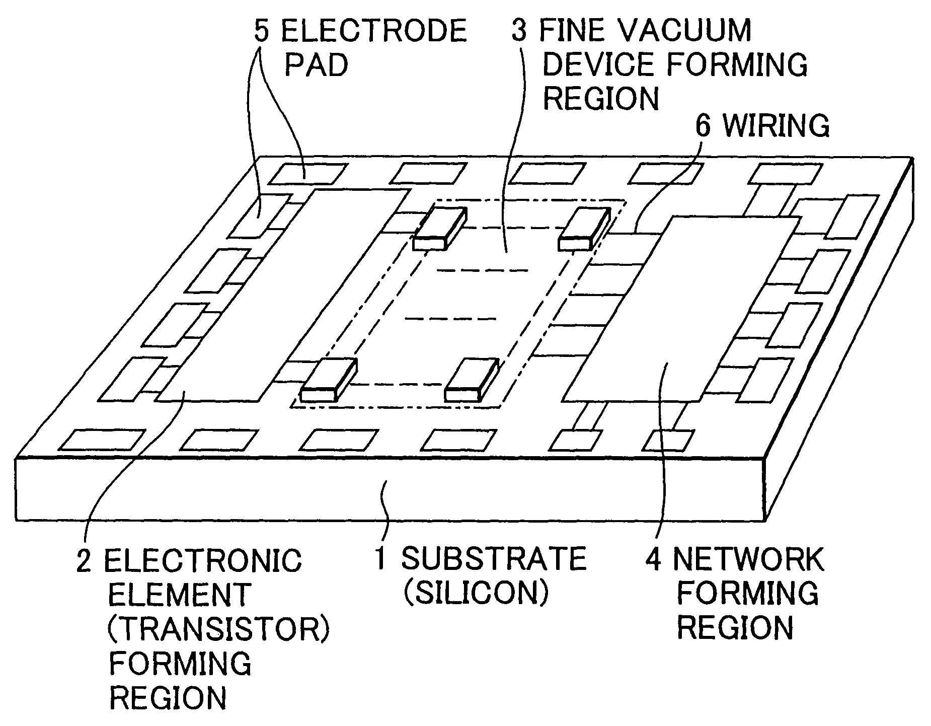
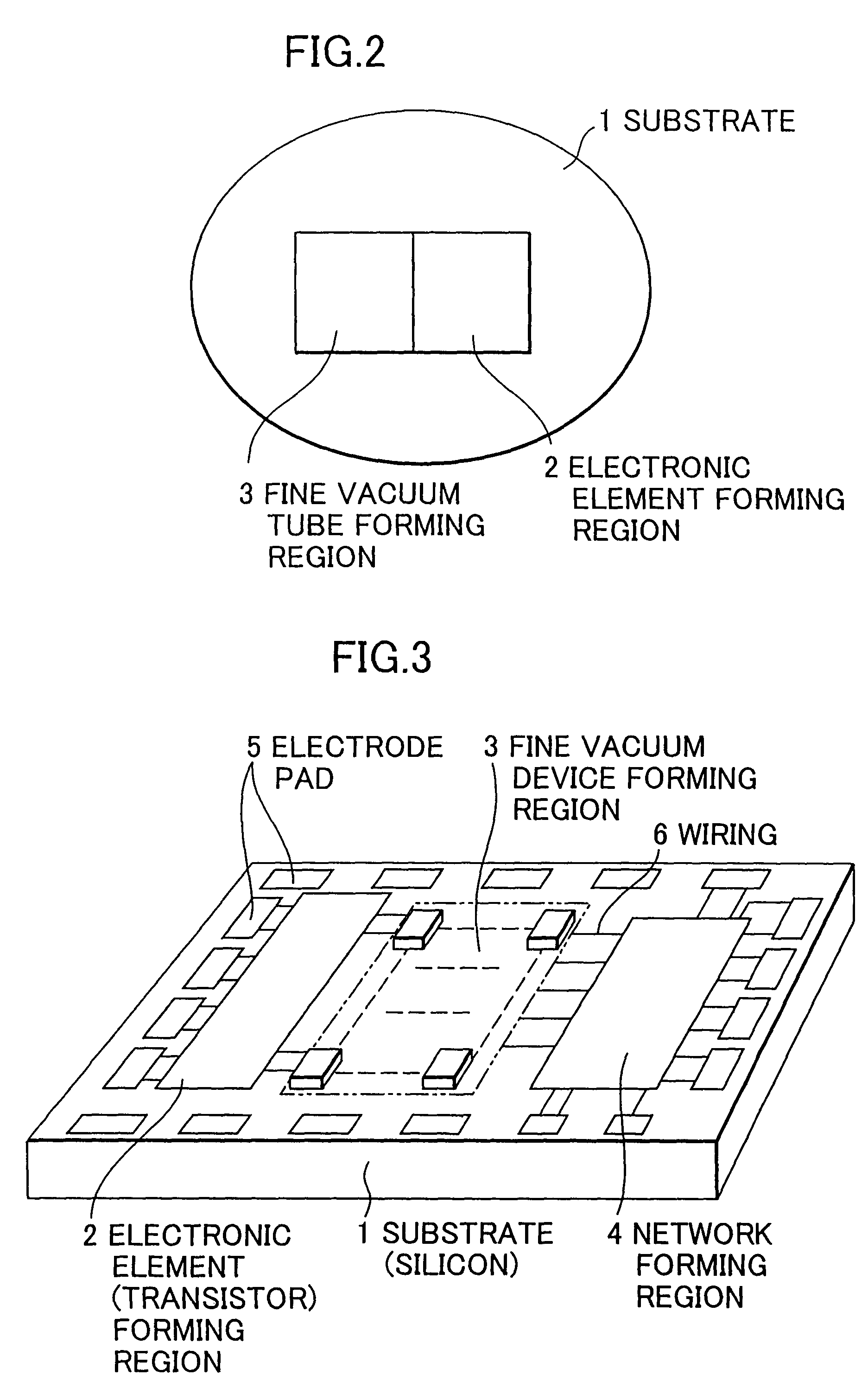
[0032]FIG. 2 is a plan view showing an example of the embodiment of this invention. In FIG. 2, electronic elements such as CMOS transistors or bipolar transistors are formed in an electronic element forming region 2 on a substrate 1 of Si or InP and the like, and a fine vacuum tube is formed in a fine vacuum tube forming region 3 by a known technique. These elements are organically connected to form an integrated circuit.

[0...


PUM


Abstract

A fine vacuum tube element and other electronic elements are integrated and formed on a semiconductor substrate, and the fine vacuum tube element and the other electronic elements transmit signals to and from each other. When integrating the vacuum tube element with the other electronic elements, a quantum effect is realized in a room temperature environment by utilizing ballistic electrons (non-scattering electrons) traveling through the vacuum, and in the integrated circuit, an A/D converter is constructed by an interference system such as a Mach-Zehnder interferometer. Also an integrated circuit of an advanced function-integrated type is provided, comprising an interference system such as a Mach-Zehnder interferometer wherein weighting of the Mach-Zehnder interferometer is constituted for image processing and signal code conversion. A very high-speed light-receiving integrated circuit for optical communication is constructed by utilizing a very high-speed optical response characteristic of electron emission of the vacuum element, and a sensor such as a magnetic/electric field sensor is constructed by utilizing a quantum effect of ballistically traveling electrons.

Description

BACKGROUND OF THE INVENTION[0001]1. Field of the Invention[0002]This invention relates to an integrated circuit and particularly to an integrated circuit that realizes higher speed, more advanced functions and reduction in the number of elements.[0003]2. Description of the Related Art[0004]The Si semiconductor integration technique has achieved satisfactory improvement in the degree of integration and speed from 2 μm to 1 μm, 0.5 μm, 0.25 μm, 0.13 μm and 0.09 μm. Moreover, some semiconductor manufacturers plan to achieve 0.065 μm. Also the exposure technique has progressed from g-line to i-line exposure to phase shift exposure and further to an excimer light source. Currently, an excimer light source plus phase shift exposure is employed.[0005]A concave mirror technique that enables construction of a miniature optical system, which was difficult to realize in the X-ray contraction projection technique, is being completed, and realization of an X-ray stepper / X-ray scanning exposure s...

Claims


Application Information

Patent Timeline
Patent Type & Authority Patents(United States)
IPC IPC(8): H01L31/00H01J1/15H01J21/00H01J21/04H01J40/12H01J40/16H01L21/822H01L27/04H02J3/00H03M1/36
CPCH03M1/361H01J21/00
Inventor MIURA, AKIRAKOBAYASHI, SHINJIHARA, HITOSHIYAKIHARA, TSUYOSHIOKA, SADAHARU
Owner YOKOGAWA ELECTRIC CORP
Why Eureka
Try Eureka