
Low dielectric constant films and manufacturing method thereof, as well as electronic parts using the same

a technology of dielectric constant and manufacturing method, which is applied in the direction of liquid/fluent solid measurement, fluid pressure measurement, peptide, etc., can solve the problems of insufficient dielectric breakdown voltage and insulation resistance, insufficient mechanical strength, and not yet put to practical use, so as to reduce leak current, increase dielectric breakdown voltage, and good heat conductivity

Inactive Publication Date: 2010-07-06
RORZE CORP
View PDF16 Cites 5 Cited by
  • Summary
  • Abstract
  • Description
  • Claims
  • Application Information

AI Technical Summary

Benefits of technology

The patent text describes the technical problem of developing a material with a low dielectric constant for use in semiconductor manufacturing processes. The text discusses various materials that have been studied, such as fluorine-added silica and polytetrafluoroethylene, but highlights the limitations of each. The text also discusses the issue of fine diamond particles containing impurities that can affect their electrical properties. The technical effect of the patent is to provide a solution for developing a low dielectric constant material with high insulation resistance and a high dielectric breakdown voltage.

Problems solved by technology

Since the silica film per se comprises two kinds of atoms of oxygen and silicon of high electronegativity, orientation polarization remains and it is insufficient as the low dielectric constant film, so that porous silica produced by a blowing method of fine particles has been studied.
However, they are insufficient in the mechanical strength and have not yet been put to practical use.
Further, while polytetrafluoroethylene as the fluororesin shown in the table has a sufficient specific dielectric constant, this can not be used since a severe condition for the required heat resistance from 300° C. to 400° C. or higher in the semiconductor manufacturing process can not be satisfied While the polyimide is a heat resistant resin, it is carbonized at 400° C. or higher and can not be used as well.
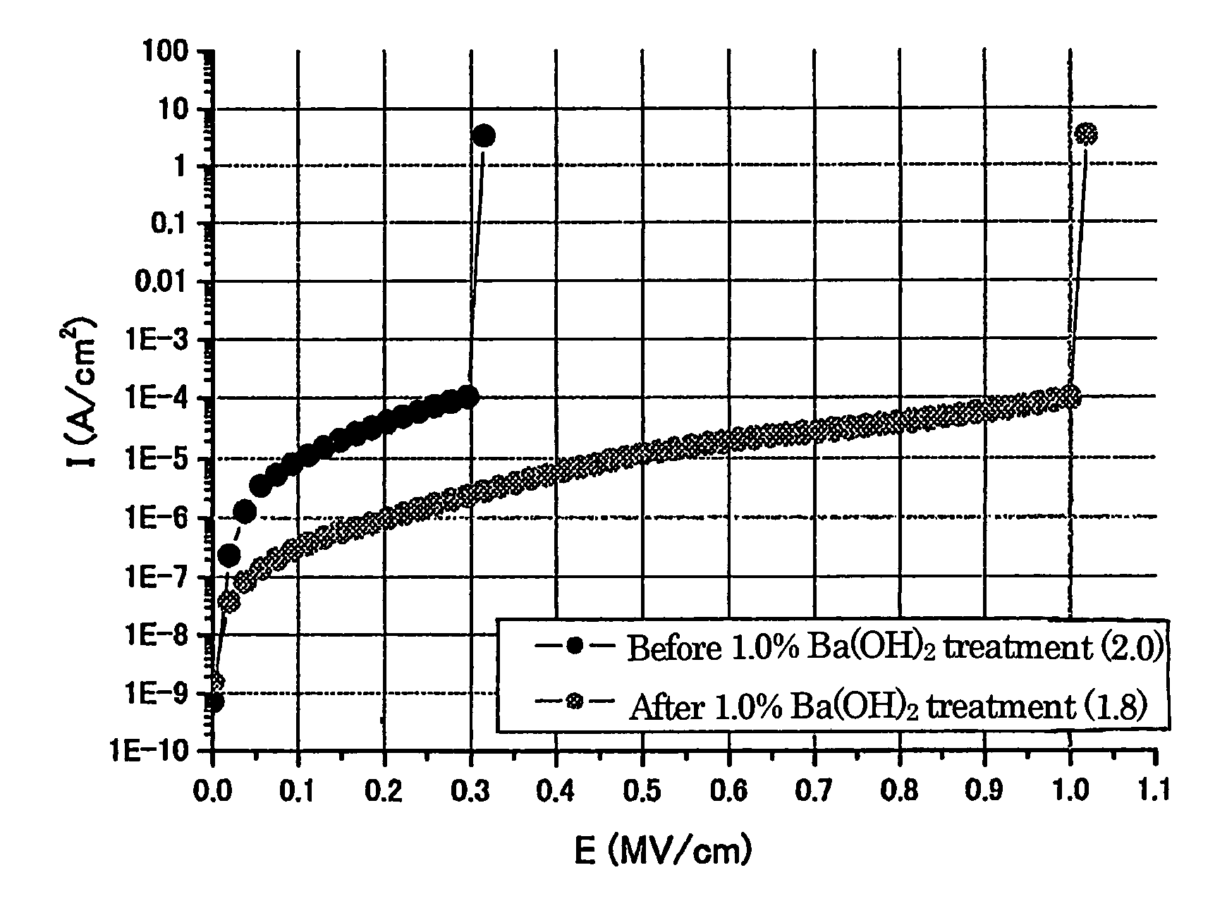
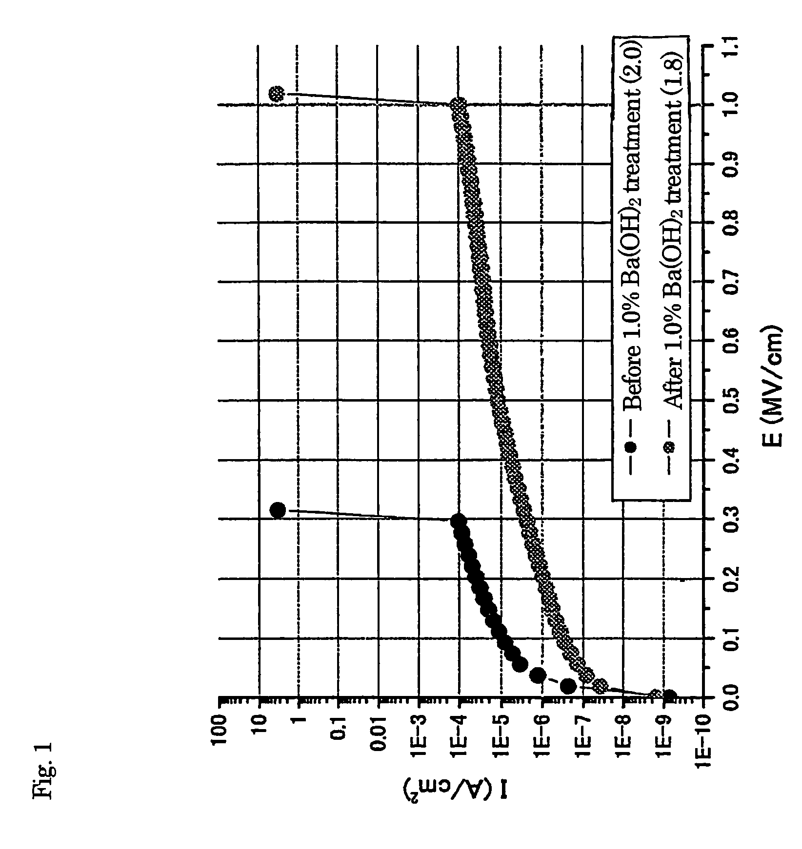
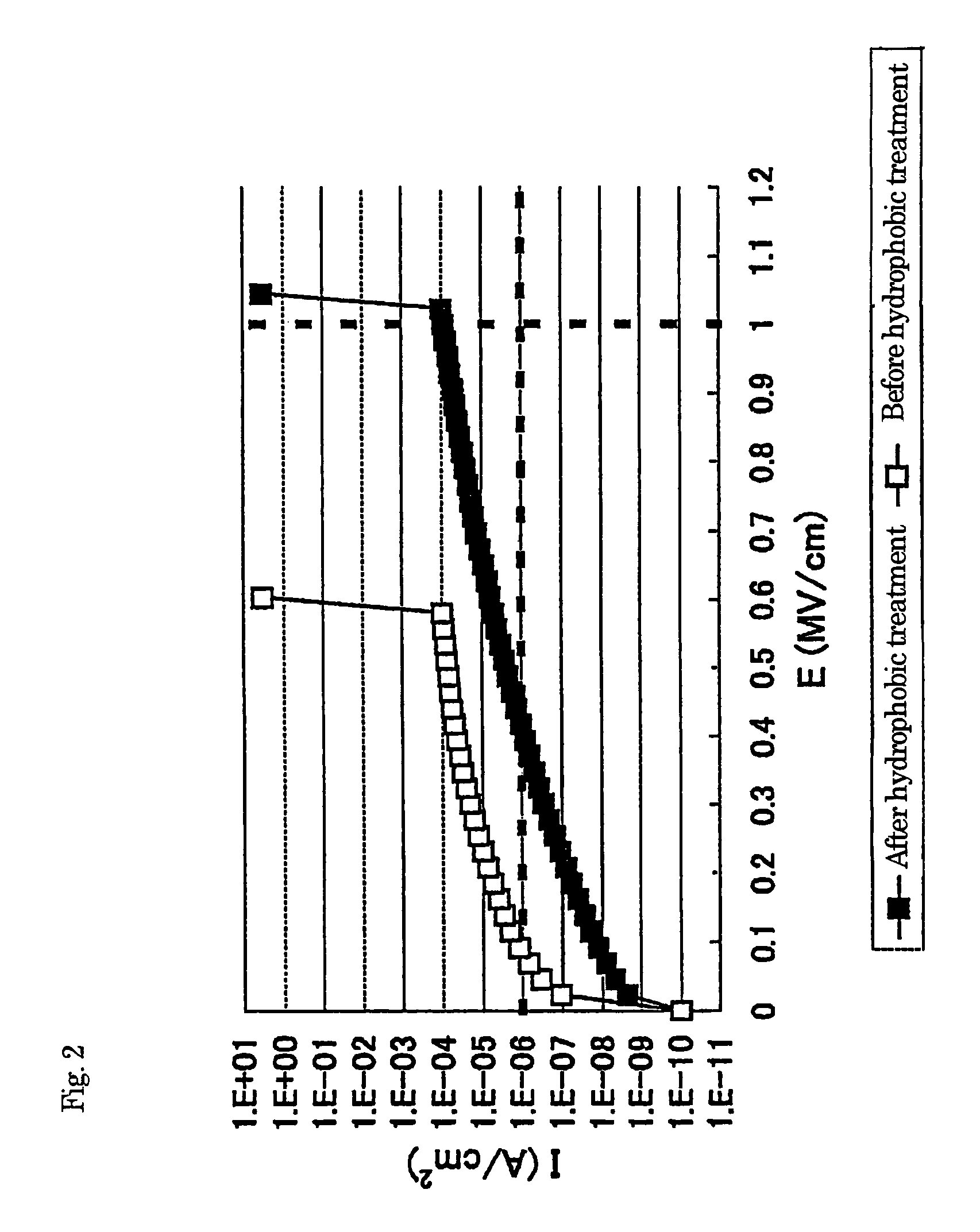
As a result of further study, it has been found that the dielectric breakdown voltage and insulation resistance are insufficient.
Accordingly, while fine diamond particles as coarse raw material are oxidized by a concentrated sulfuric acid or concentrated nitric acid to remove the impurities, this is not yet sufficient and, while various methods such as increase of the oxidation temperature in the acid treatment has been studied, a sufficiently high electric resistance value and a sufficiently high dielectric breakdown voltage have not yet been attained.
That is, it is considered that leak current is caused and the dielectric breakdown voltage is not increased as well by the water molecules having affinity with the hydrophilic groups and impurities contained in a trace amount.

Method used


Image

  • Low dielectric constant films and manufacturing method thereof, as well as electronic parts using the same
  • Low dielectric constant films and manufacturing method thereof, as well as electronic parts using the same
  • Low dielectric constant films and manufacturing method thereof, as well as electronic parts using the same

Examples


example 1

Preparation of Colloidal Solution

[0059]In pure water in a beaker made of quartz, 5% by weight of purified fine diamond particles and 1% by weight of polyethylene glycol 600 were charged and the beaker was dipped in an ultrasonic wave tank and sufficiently dispersed for one hour to obtain a gray viscous dispersion liquid.

[0060]A thoroughly cleaned silicon substrate was placed on a spindle of a spin coater, the colloidal solution described above was poured downward and the substrate was rotated at 1500 rpm to uniformly coat the same by a centrifugal force.

[0061]The silicon substrate coated with a liquid of fine diamond particles was air-dried to form a film and then placed on a hot plate at 300° C. and dried for one hour.

[0062]The silicon substrate with the fine diamond particle film was placed in a vessel and tightly dosed and put to interparticle crosslinking by exposure to a vapor of 1% hexachlorodisiloxane dissolved in dichloromethane at an ambient temperature for one hour and the...

example 2

[0066]Experiment was conducted in the same procedures except for conducting the metal salt treatment with 0.17% calcium hydroxide instead of 1% barium hydroxide in Example 1. The film thickness was 430 nm. As a result, it has been found that the dielectric breakdown voltage improved from 0.86 MV / cm to 1.05 MV / cm and the leak current at 0.82 MV / cm decreased from 1×10⁻⁴ A / cm2 to 7×10⁻⁵ A / cm2 also by treatment with calcium.

[0067]Examples of the invention are to be described below but the invention is not limited only to the examples.

example 3

Preparation of Colloidal Solution

[0068]In pure water in a beaker made of quartz, 5% by weight of purified fine diamond particles and 1% by weight of polyethylene glycol 600 were charged and the beaker was dipped in an ultrasonic wave tank and sufficiently dispersed for one hour to obtain a gray viscous dispersion liquid.

[0069]A thoroughly cleaned silicon substrate of about 20 mm square applied with a hydrophilic surface treatment was placed on a spindle of a spin coater, the colloidal solution described above was poured downward and the substrate was rotated at 1500 rpm to uniformly coat the same by a centrifugal force.

[0070]The silicon substrate coated with a liquid of fine diamond particles was air-dried to form a film and then placed on a hot plate at 300° C. and dried for one hour.

[0071]The silicon substrate with the fine diamond particle film was placed in a tightly dosed vessel and put to inter-particle crosslinking by exposure to a vapor of 1% hexachlorodisiloxane (HCDS) diss...


PUM

PropertyMeasurementUnit
dielectric constantaaaaaaaaaa
thicknessaaaaaaaaaa

Abstract

While a fine porous diamond particle film has been known as a high heat resistant and low dielectric constant film and also has high mechanical strength and heat conductivity, and is expected as an insulating film for multi-layered wirings in semiconductor integrated circuit devices, it is insufficient in current-voltage characteristic and has not yet been put into practical use. According to the invention, by treating the fine porous diamond particle film with an aqueous solution of a salt of a metal such as barium and calcium, the carbonate or sulfate of which is insoluble or less soluble, and a hydrophobic agent such as hexamethyl disilazane or triethyl monochloro silane, as well as a reinforcing agent containing one of dichlorotetramethyl disiloxane or dimethoxytetramethyl disiloxane, thereby capable of putting the dielectric breakdown voltage and the leak current within a specified range of a practical standard.

Description

TECHNICAL FIELD[0001]The present invention concerns a low dielectric constant thin film as an insulating film of a porous structure in which fine diamond particles are bonded, and a manufacturing method thereof, as well as an electronic part such as a semiconductor integrated circuit device of high integration degree and high speed operation type using the same.BACKGROUND ART[0002]Among semiconductor integrated circuit devices, particularly in super LSI devices, delay of signals passing through wirings prepared in devices gives rise to a significant problem along with lowering of power consumption as the wirings become finer and are more integrated. Particularly, in a high speed logic device, RC delay due to the resistance and the distribution capacity of wirings results in most prominent subject and, among all it is necessary to use a material of low dielectric constant for inter-wiring insulating materials in order to decrease the distribution capacity.[0003]Heretofore, as an insu...

Claims


Application Information

Patent Timeline
Patent Type & Authority Patents(United States)
IPC IPC(8): H01L21/31H01L21/314
CPCH01L21/3146H01L21/02115H01L21/02175H01L21/02282H01L21/02203H01L21/02126H01L21/02216H01L21/31
Inventor SAKURAI, TOSHIOTAKAHAGI, TAKAYUKISAKAUE, HIROYUKISHINGUBARA, SHOSOTOMIMOTO, HIROYUKI
Owner RORZE CORP
Learn More