
Photon logic gates

a logic gate and photon technology, applied in the field of photon logic gates, can solve the problems of bulky optical logic gates using linear optics such as mirrors, splitters, and fundamental limitations of electronic transistors

Inactive Publication Date: 2010-07-13
GWANGJU INST OF SCI & TECH +1
View PDF6 Cites 3 Cited by
  • Summary
  • Abstract
  • Description
  • Claims
  • Application Information

AI Technical Summary

Benefits of technology

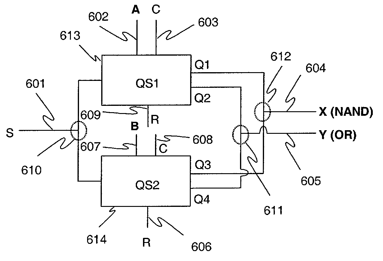
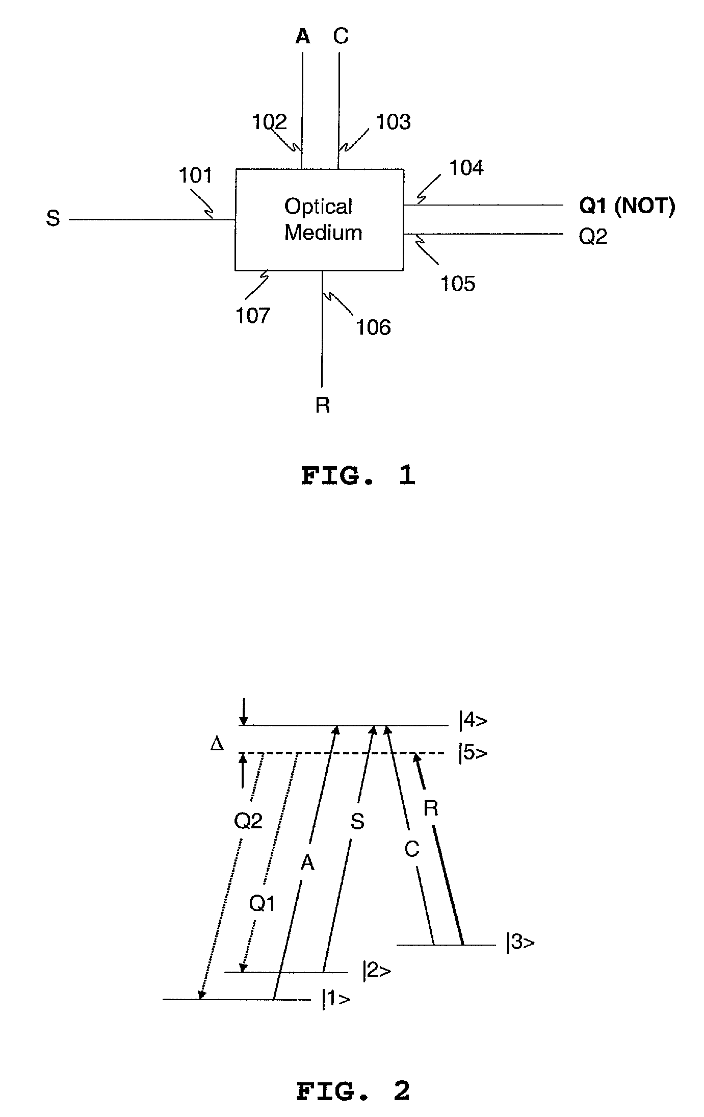
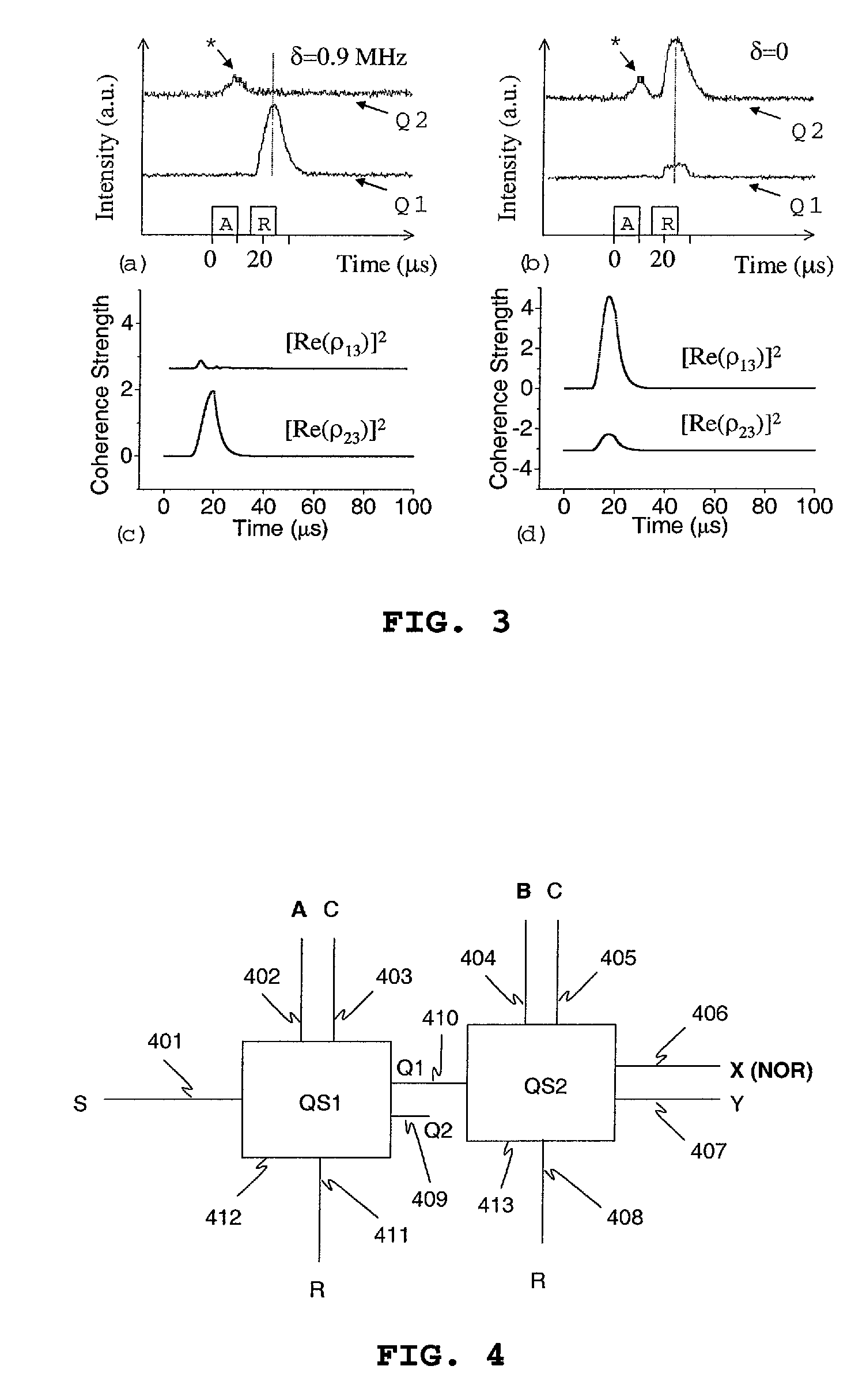
[0007]The primary object of the present invention is to provide a method and an apparatus of photon logic gates based on quantum switching phenomenon. The photon logic gates should overcome limitations of the conventional optical logic gates in operational speed and size. The main feature of the photon logic gates is using quantum optics of EIT and quantum switch for multiple gate function in one physical gate composed of three (four)-color lasers interacting with a nonlinear optical medium via optical waveguides or free space. As shown in the quantum switch (Ham, U.S. Pat. No. 6,628,453), the operational bandwidth of the present photon logic gates is not limited by the population relaxation time or carrier's lifetime. Main advantage of the present invention is not only for all-optical digital processing but also for quantum interface in a quantum network composed of quantum computers. Briefly described, a system of the photon logic gates of the present invention is provided by a single or multiply connected quantum switches composed of nonlinear optical medium and at least four coherent laser beams. The nonlinear optical medium of the quantum switch is composed of at least four-energy levels. Three of them should be closely spaced on the ground states, and the last one should be an excited state. The frequencies of the laser beams of A, C, and S are resonant respectively to the transitions from the three ground states |1>, |2>, and |3> to the excited state |4> of the nonlinear optical medium: see FIGS. 1 and 2. The laser beam R is used as a probe for nondegenerate four-wave mixing processes to generate the outputs Q1 or Q2. The nondegenerate four-wave mixing output Q1 and / or Q2 can be used as an input(s) to the second / third nonlinear medium to configure a photon logic gate. The output direction of the Q1 and Q2 is physically separated, so that the quantum switch acts as an optical router: Ham, Applied Physics Letters Vol. 85, pp. 893-895 (2004). Each laser beam can be guided by an optical waveguide made of hetero-structured quantum wells, photonic bandgap crystals, silicon on insulator, or surface plasmon. The optical waveguide is not part of the current invention. By connecting two quantum switches in series or in parallel it performs the Boolean logic: NOT, NAND, AND, OR, XOR, and NOR. The photon logic gates can be extended for scalability purposes by an optical waveguide, and the traveling time between two photon logic gates is negligible.
is not only for all-optical digital processing but also for quantum interface in a quantum network composed of quantum computers. Briefly described, a system of the photon logic gates of the present invention is provided by a single or multiply connected quantum switches composed of nonlinear optical medium and at least four coherent laser beams. The nonlinear optical medium of the quantum switch is composed of at least four-energy levels. Three of them should be closely spaced on the ground states, and the last one should be an excited state. The frequencies of the laser beams of A, C, and S are resonant respectively to the transitions from the three ground states |1>, |2>, and |3> to the excited state |4> of the nonlinear optical medium: see FIGS. 1 and 2. The laser beam R is used as a probe for nondegenerate four-wave mixing processes to generate the outputs Q1 or Q2. The nondegenerate four-wave mixing output Q1 and / or Q2 can be used as an input(s) to the second / third nonlinear medium to configure a photon logic gate. The output direction of the Q1 and Q2 is physically separated, so that the quantum switch acts as an optical router: Ham, Applied Physics Letters Vol. 85, pp. 893-895 (2004). Each laser beam can be guided by an optical waveguide made of hetero-structured quantum wells, photonic bandgap crystals, silicon on insulator, or surface plasmon. The optical waveguide is not part of the current invention. By connecting two quantum switches in series or in parallel it performs the Boolean logic: NOT, NAND, AND, OR, XOR, and NOR. The photon logic gates can be extended for scalability purposes by an optical waveguide, and the traveling time between two photon logic gates is negligible.

Problems solved by technology

However, there have been fundamental limitations in electronic transistors in such a way of gate-width dependent switching time and electromagnetic-interference-limited operational bandwidth.
A bulky optical logic gate using linear optics such as mirrors and beam splitters has been applied.
The linear optics based optical gate is of course lacks efficiency due to bulky size.
Therefore, the conventional optical switching time should be fundamentally limited by the carriers' lifetime, where it is sub-nanosecond.
1271-3 (1997)), total estimated power and size for a potential optical CPU composed of just million units of SOA reaches at several ˜100 kW and several square meters, respectively, which is never practical.
The quantum interference-based refractive index change can result in strong spin coherence excitation on the closely spaced states and absorption cancellation.

Method used


Image

  • Photon logic gates
  • Photon logic gates
  • Photon logic gates

Examples


Embodiment Construction

[0016]To gain a better understanding reference is now made to the drawings which illustrate the preferred embodiments of the invention. FIG. 1 describes a photon logic gate, NOT, where a single quantum switch is used. Letters R, S, C, A, Q1, and Q2 stand for laser beams at different frequencies of ωR, ωS, ωC, ωA, ωQ1, and ωQ2, respectively. The numbers from 101 to 106 stand for both laser beams and optical waveguide used for the laser beams. The number 107 stands for a nonlinear optical medium. According to the quantum switch theory (Physical Review Letters. Vol. 84, pp. 4080-4083 (2000), and Applied Physics Letters, Vol. 78, pp. 3382-3384 (2001); Applied Physics Letters, Vol. 85, pp. 893-895 (2004); U.S. Pat. No. 6,628,453 (2003)), the output Q1 (104) is always OFF whenever the logical input beam A (102) is switched ON, and vice versa. Here it should be noted that the laser beams C and R may be continuous if the detuning Δ is not zero: the detuning Δ is shown in FIG. 2. If the detu...


PUM

PropertyMeasurementUnit
power consumptionaaaaaaaaaa
frequencyaaaaaaaaaa
energy levelaaaaaaaaaa

Abstract

A system, method, and apparatus for photon logic gates based on quantum switch, where a single or multiple quantum switches are utilized for dark resonance interactions in which three-color lasers interact with a four-level or five-level nonlinear optical medium composed of three ground states and one or two excited states through nondegenerate four-wave mixing processes. The photon logic mechanism is based on combination of single or multiple dark resonance-induced two-photon coherence swapping among the three closely spaced ground states through optical transitions via a common excited state. The two-photon coherence induced on the ground states is optically detected via nondegenerate four-wave mixing processes. The nondegenerate four-wave mixing generation is enhanced owing to dark resonance or electromagnetically induced transparency. The gating time and bandwidth of the present photon logic gate method is not limited by population relaxation time or carrier's lifetime, but phase decay time, where the phase decay time in general much faster than the population decay time in solids or semiconductors.

Description

TECHNICAL FIELD[0001]The present invention relates to a method and apparatus for photon logic gates using quantum switch(es).BACKGROUND ART[0002]A logic gate is generally used for logical operations in data processing using one more logic inputs to produce a single output. The logic is normally referred to Boolean logic such as NOT, OR, NOR, XOR, XNOR, AND, and NAND. For an electronic central processing unit (CPU) the logic gate acts as a basic unit to perform computing operations. Due to the increasing demand for faster processing ability, the CPU has been exponentially evolved up to now 3.7 GHz in 2006 according to the Moore's law since mid 1970s. However, there have been fundamental limitations in electronic transistors in such a way of gate-width dependent switching time and electromagnetic-interference-limited operational bandwidth. To overcome such fundamental limitations, optical logic gates have been studied for last several decades. On the contrary, as a counterpart of elec...

Claims


Application Information

Patent Timeline
Patent Type & Authority Patents(United States)
IPC IPC(8): G02F3/00
CPCG02F3/00G06E1/00G06N99/002B82Y10/00G06N10/00G02B6/35
Inventor HAM, BYOUNG SEUNG
Owner GWANGJU INST OF SCI & TECH
Learn More