Graphene-diamond hybrid material and method for preparing same using chemical vapor deposition
a technology of diamonds and hybrid materials, applied in the direction of crystal growth process, polycrystalline material growth, transportation and packaging, etc., can solve the problem of inability to synthesize graphen
- Summary
- Abstract
- Description
- Claims
- Application Information
AI Technical Summary
Benefits of technology
Problems solved by technology
Method used
Image
Examples
example 1
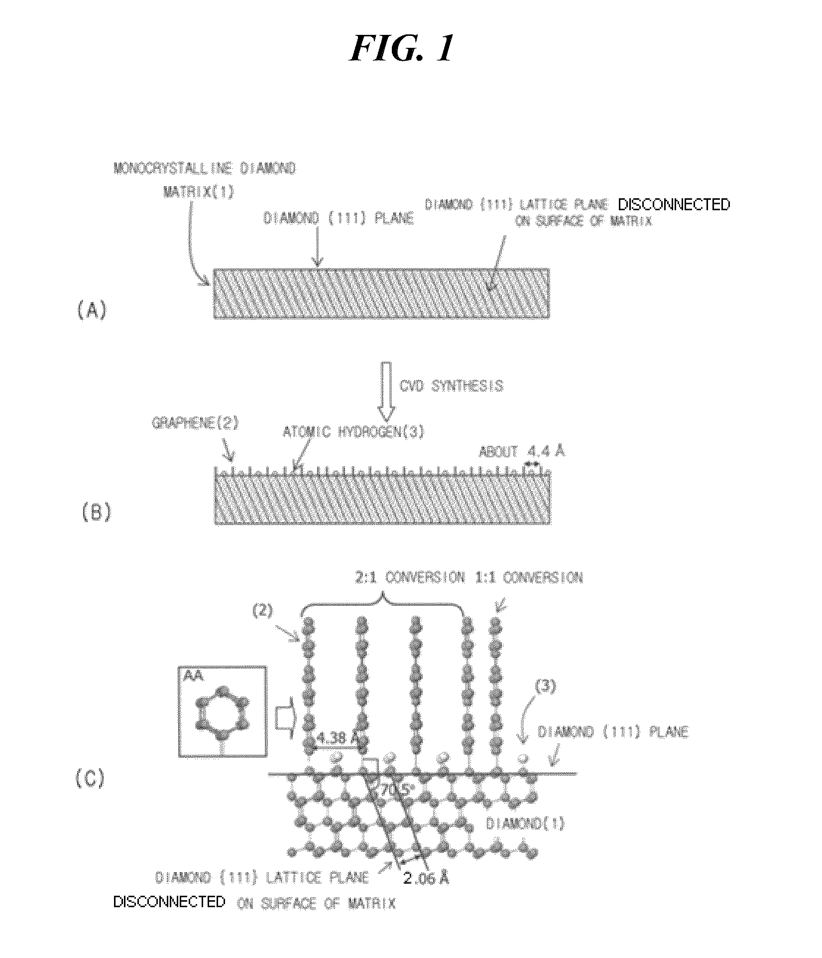
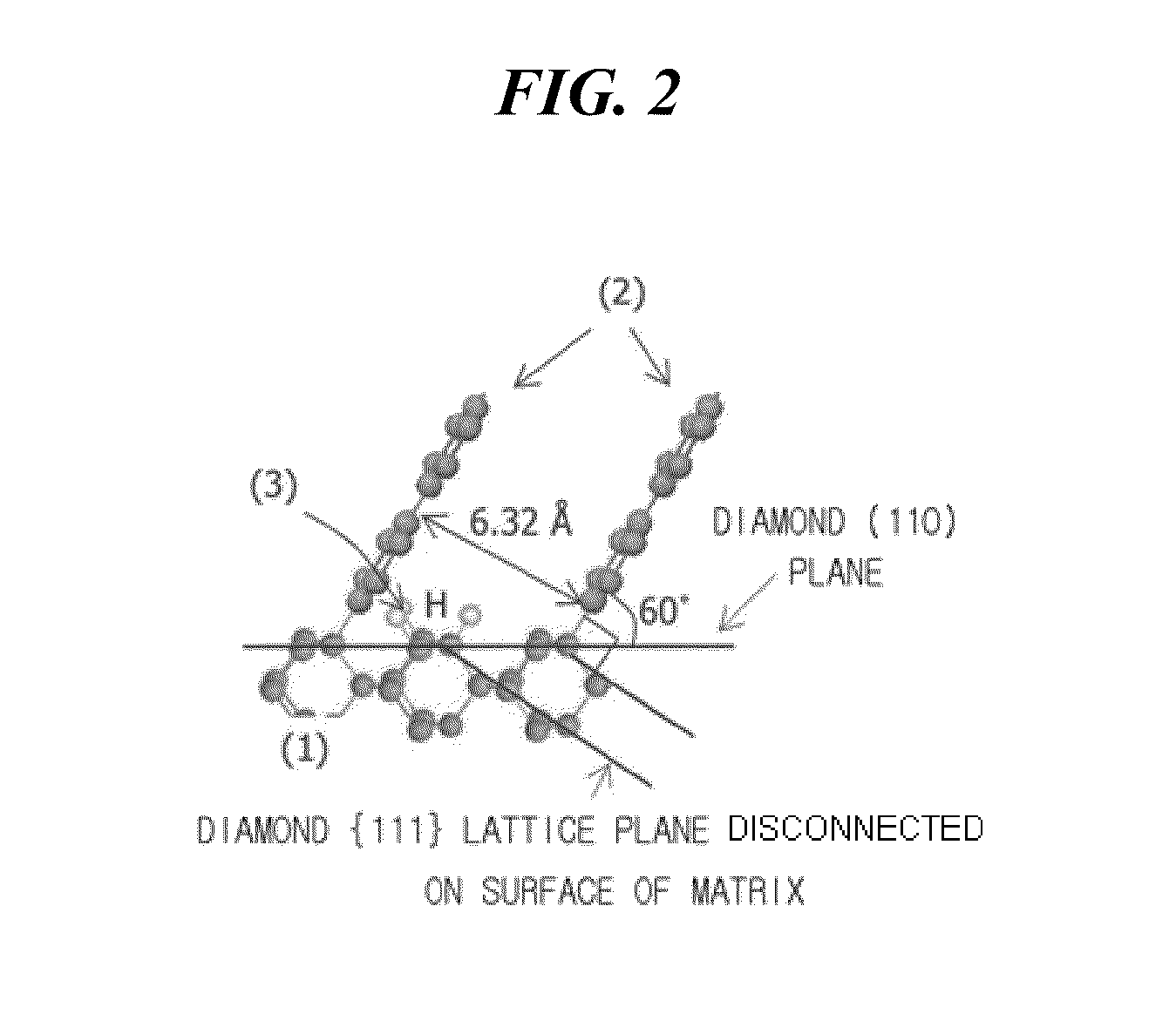
[0058]Graphene was synthesized using a method shown in FIG. 1. (110) monocrystalline diamond having {111} lattice planes disconnected on the surface thereof was used as a matrix. Direct-current plasma was used in CVD synthesis. 20% of methane (CH4) and 80% of hydrogen (H2) were used as reaction gases. The synthesis of graphene was conducted under the conditions of a pressure of 1 Torr, a gas flow rate of 200 sccm, a matrix temperature of about 70° C. and a synthesis time of 30 minutes.
[0059]After the synthesis of graphene, a diamond matrix sample was collected and then observed by a high resolution transmission electron microscope (HRTEM). As a result, it was observed that the layers of graphene were vertically grown to a length of several nanometers (nm) while meeting with the surface of the matrix at an angle of 60°. When measured at a position spaced apart from the interface between diamond and graphene by 2 nm, the average interplanar spacing between the layers of graphene was 3...
example 2
[0060]Graphene was synthesized using a method shown in FIG. 3. First, a silicon substrate having a thickness of 1 mm was coated with a nanocrystalline diamond film using a direct-current plasma diamond synthesis apparatus. In this case, the coating of the silicon substrate was conducted under the conditions of a gas composition including 10% methane (CH4) and 90% hydrogen (H2), a pressure of 100 Torr, a gas flow rate of 200 sccm, a substrate temperature of about 70° C. and a synthesis time of 1 hour. The thickness of the nanocrystalline diamond film applied on the silicon substrate was 10 μm. As the results of Raman-analysis of the nanocrystalline diamond film, the nanocrystalline diamond film exhibited the properties of typical nanocrystalline diamond film.
[0061]Subsequently, an experiment for synthesizing graphene on the silicon substrate coated with the nanocrystalline diamond film was conducted. In this case, the synthesis of the graphene was conducted under the conditions of a ...
example 3
[0063]Graphene was synthesized using a method shown in FIG. 4. A nanocrystalline diamond film having a crystal grain size of 20˜30 nm, a thickness of 10 μm and a diameter of 4 inches formed on a silicon substrate having a thickness of 1 mm, which was formed using the same method as in Example 2, was used as a matrix.
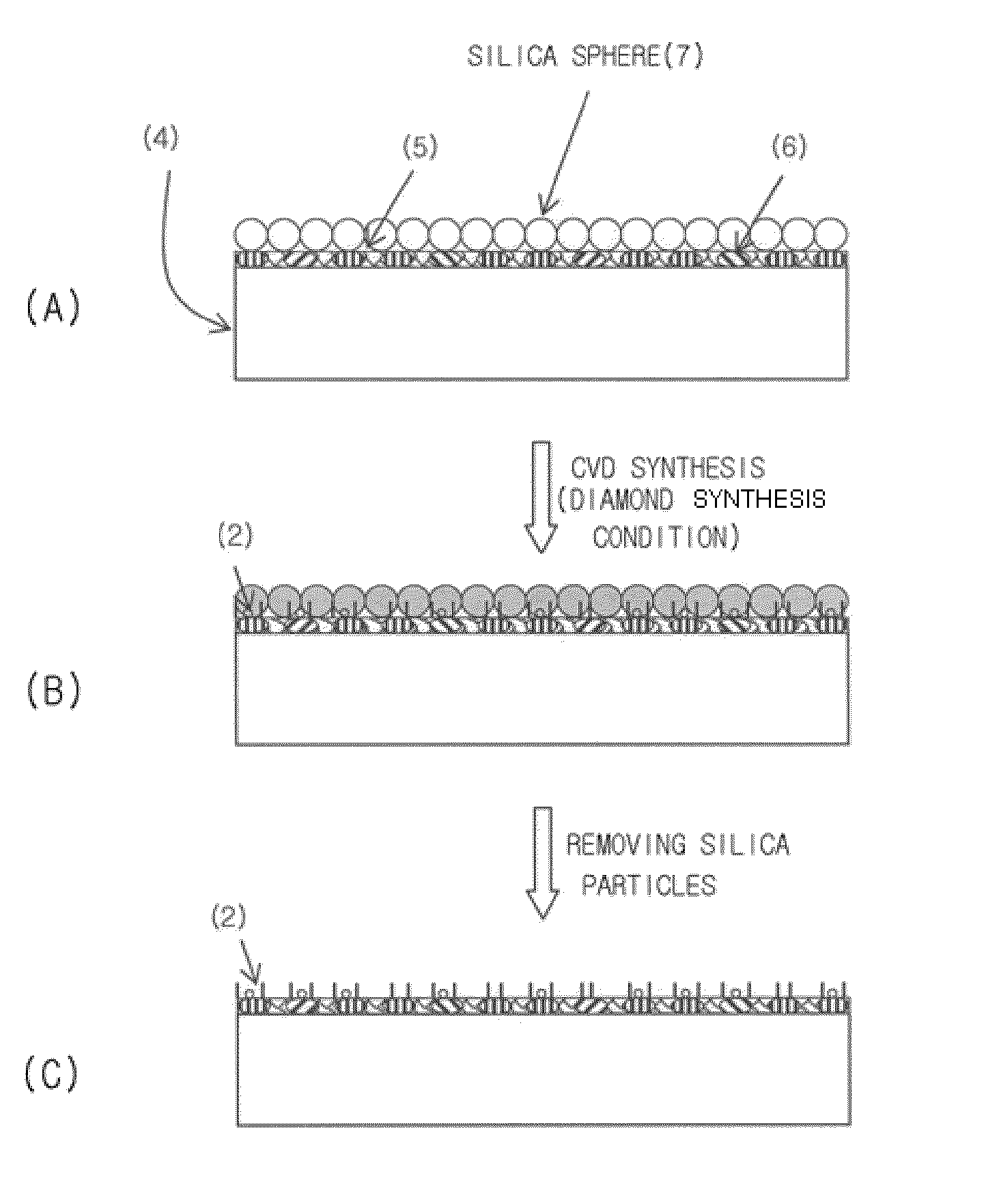
[0064]Silica spheres having a size of about 10 μm were closely placed on the nanocrystalline diamond film and then the synthesis of graphene was performed using a multi-cathode direct-current plasma diamond synthesis apparatus. In this case, the synthesis of the graphene was conducted under the conditions of a gas composition including 10% methane (CH4) and 90% hydrogen (H2), a pressure of 100 Torr, a gas flow rate of 200 sccm, a silica sphere surface temperature of about 700° C. and a synthesis time of 30 minutes.
[0065]After the synthesis of graphene, a sample was collected and then analyzed using a high resolution transmission electron microscope (HRTEM). As a result, ...
PUM
| Property | Measurement | Unit |
|---|---|---|
| pressure | aaaaa | aaaaa |
| temperature | aaaaa | aaaaa |
| pressure | aaaaa | aaaaa |
Abstract
Description
Claims
Application Information


