
Tunnel field-effect transistor with narrow band-gap channel and strong gate coupling

a field-effect transistor and tunnel-effect technology, applied in semiconductor devices, diodes, electrical devices, etc., can solve the problems of inability to achieve fast switching at low operation voltage for future nanometer devices, inability to achieve fast switching at low operation voltage, and inability to achieve ultra thin body mosfet on soi or finfet to achieve close to, but not below, the limit of 60 mv/decade, etc., to achieve the effect of reducing leakage curren

Inactive Publication Date: 2010-10-12
TAIWAN SEMICON MFG CO LTD
View PDF13 Cites 53 Cited by
  • Summary
  • Abstract
  • Description
  • Claims
  • Application Information

AI Technical Summary

Benefits of technology

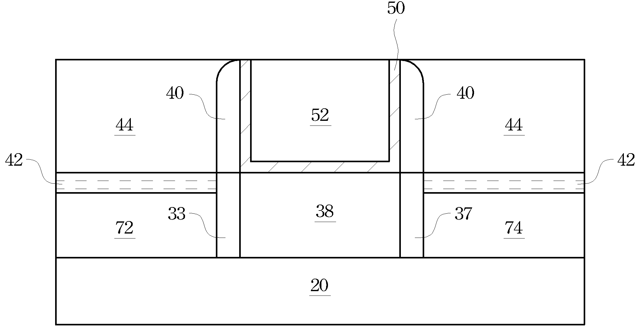
The present invention relates to a semiconductor device and a method for forming the same. The semiconductor device includes a low energy band-gap layer, a gate dielectric, a gate electrode, and source / drain regions. The source / drain regions have a higher conductivity type than the low energy band-gap layer. The method includes forming a dummy gate stack, using it as a mask to recess the low energy band-gap layer, and filling the recesses with a semiconductor material to form semiconductor regions with opposite conductivity types. The semiconductor device and method provide improved performance and reliability.

Problems solved by technology

This limitation is due to the drift-diffusion transport mechanism of carriers.
For this reason, existing MOS devices typically cannot switch faster than 60 mV / decade at room temperatures.
However, even with better gate control over the channel, an ultra thin body MOSFET on SOI or FinFET can only achieve close to, but not below, the limit of 60 mV / decade.
With such a limit, faster switching at low operation voltages for future nanometer devices cannot be achieved.
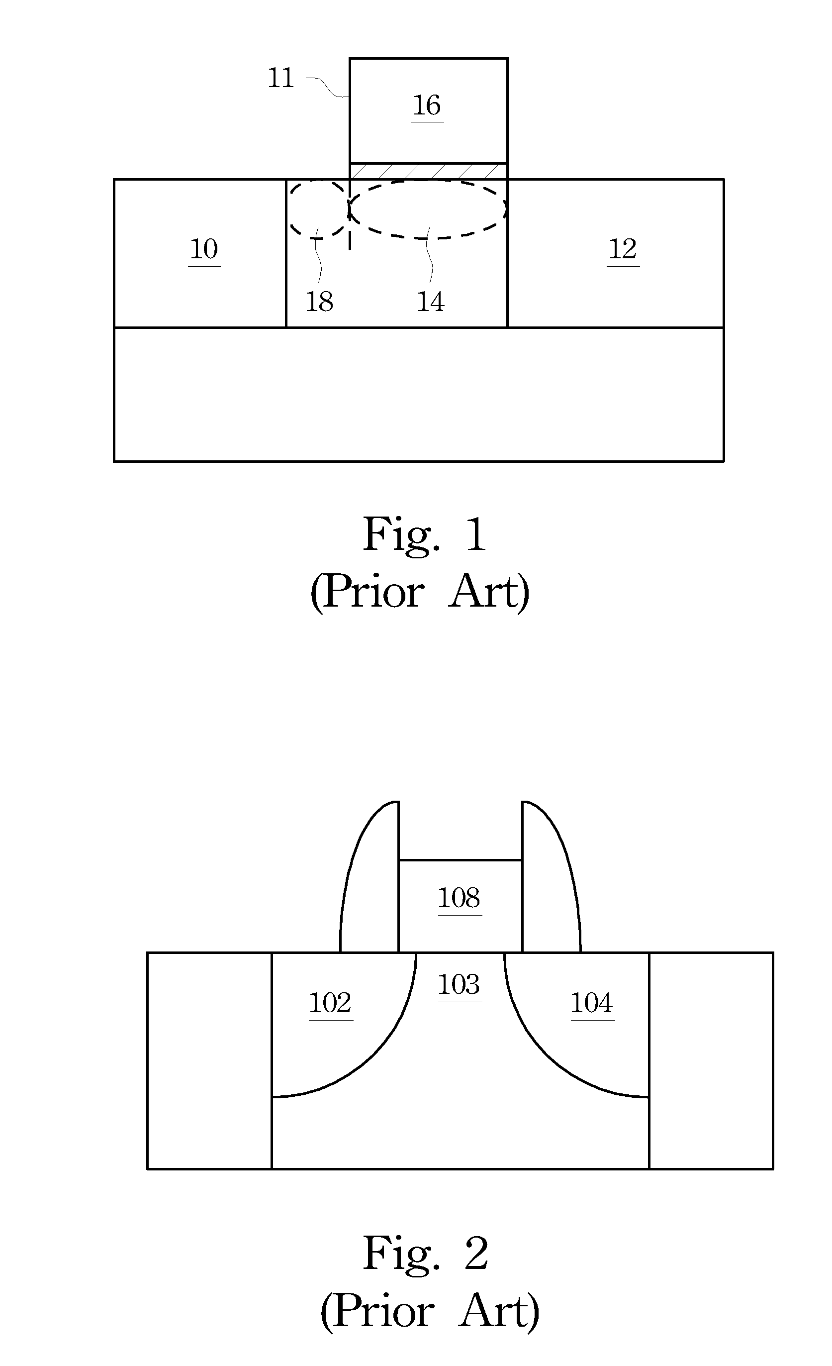
Further, although it is capable of ultra-fast switching by avalanche mechanism, the critical width of the offset region 18 is sensitive to alignment errors between the gate and the source / drain.
Furthermore, the avalanche mechanism of the I-MOS device is temperature sensitive, and temperature variations also lead to variations in sub-threshold swing.
However, such a structure can only improve the on-currents of n-channel tunnel FET devices, while the on-currents of p-channel tunnel FET devices are not improved.

Method used


Image

  • Tunnel field-effect transistor with narrow band-gap channel and strong gate coupling
  • Tunnel field-effect transistor with narrow band-gap channel and strong gate coupling
  • Tunnel field-effect transistor with narrow band-gap channel and strong gate coupling

Examples


first embodiment

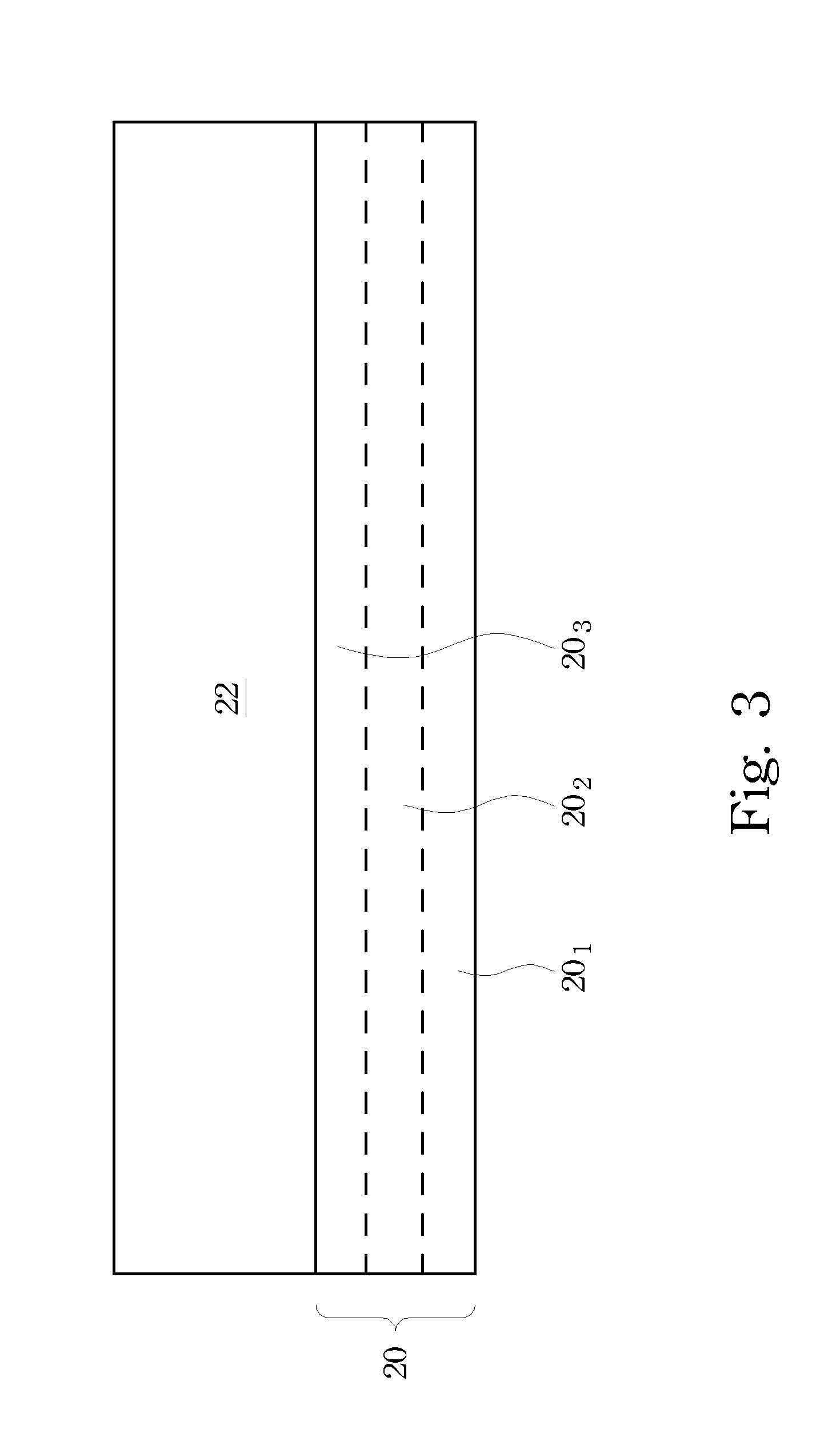
[0030]the present invention is provided in FIGS. 3 through 10. Referring to FIG. 3, substrate 20 is provided. In an embodiment, substrate 20 is a bulk substrate comprising a single crystalline semiconductor material, such as silicon, or a compound semiconductor material. In other embodiments, substrate 20 may include more than one semiconductor layer. For example, substrate 20 may have a silicon-on-insulator or silicon-on-carbide structure, including silicon layer 203 on insulator layer 202. Insulator layer 202 may further be located on semiconductor layer 201. In yet other embodiments, substrate 20 includes an insulator.

[0031]Low (energy) band-gap layer 22 is formed over substrate 20. Throughout the description, the term “low band-gap” refers to band-gaps lower than the band-gap of silicon (1.12 eV). In the preferred embodiment, low band-gap layer 22 is formed of silicon germanium (SiGe). In other embodiments, other semiconductor materials having low band-gaps, such as Ge, GaAs, In...


PUM


Abstract

A semiconductor device and the methods of forming the same are provided. The semiconductor device includes a low energy band-gap layer comprising a semiconductor material; a gate dielectric on the low energy band-gap layer; a gate electrode over the gate dielectric; a first source / drain region adjacent the gate dielectric, wherein the first source / drain region is of a first conductivity type; and a second source / drain region adjacent the gate dielectric. The second source / drain region is of a second conductivity type opposite the first conductivity type. The low energy band-gap layer is located between the first and the second source / drain regions.

Description

TECHNICAL FIELD[0001]This invention relates generally to semiconductor devices, and more specifically to tunnel field-effect transistors formed of gated p-i-n diodes.BACKGROUND[0002]The metal-oxide-semiconductor (MOS) is a dominating technology for integrated circuits at 90 nm technology and beyond. A MOS device can work in three regions, depending on gate voltage Vg and source-drain voltage Vds, linear, saturation, and sub-threshold regions. The sub-threshold region is a region where Vg is smaller than the threshold voltage Vt. The sub-threshold swing represents the easiness of switching the transistor current off and thus is an important factor in determining the speed of a MOS device. The sub-threshold swing can be expressed as a function of m*kT / q, where m is a parameter related to capacitance. The sub-threshold swing of a typical MOS device has a limit of about 60 mV / decade (kT / q) at room temperature, which in turn sets a limit for further scaling of operation voltage VDD and t...

Claims


Application Information

Patent Timeline
Patent Type & Authority Patents(United States)
IPC IPC(8): H01L29/161H01L29/78
CPCH01L29/66356H01L29/7391H01L29/66545
Inventor BHUWALKA, KRISHNA KUMARGOTO, KEN-ICHI
Owner TAIWAN SEMICON MFG CO LTD
Learn More