Phase change memory cell employing a GeBiTe layer as a phase change material layer, phase change memory device including the same, electronic system including the same and method of fabricating the same

a phase change memory and material layer technology, applied in semiconductor devices, digital storage, instruments, etc., can solve the problems of reducing the power consumption of a write, limiting the write speed (program speed) of the phase change memory device employing the gesbte layer, and difficult to improve the integration density of the phase change memory devi

Active Publication Date: 2010-10-19
SAMSUNG ELECTRONICS CO LTD
View PDF110 Cites 28 Cited by
  • Summary
  • Abstract
  • Description
  • Claims
  • Application Information

AI Technical Summary

Benefits of technology

[0019]Additional embodiments of the invention include a method of fabricating a phase change memory cell that is capable of increasing an electrical programming speed and decreasing a reset current. The method includes forming a lower interlayer insulating layer on a semiconductor substrate and forming a first electrode in the lower interlayer insulating layer. A phase change material layer contacting the first electrode and a second electrode stacked on the phase change material layer are formed on the lower interlayer insulating layer. The phase change material layer is formed of one of an undoped GeBiTe layer having a composition ratio within a range surrounded by four points (A1(Ge21.43, Bi16.67, Te61.9), A2(Ge44.51, Bi0.35, Te55.14), A3(Ge59.33, Bi0.5, Te40.17) and A4(Ge38.71, Bi16.13, Te45.16)) represented by coordinates on a triangular composition diagram having vertices of Ge, Bi and Te, a doped GeBiTe layer containing an impurity and having a composition ratio within a range surrounded by four points (D1(Ge10, Bi20, Te70), D2(Ge30, Bi0, Te70), D3(Ge70, Bi0, Te30) and D4(Ge50, Bi20, Te30)) represented by coordinates on the triangular composition diagram, and a doped GeTe layer containing an impurity and having a composition ratio corresponding to coordinates on a straight line between the points D2 and D3. An upper interlayer insulating layer is formed on the substrate having the phase change material layer and the second electrode. The upper interlayer insulating layer is patterned to form a bit line contact hole exposing the second electrode. A bit line electrically connected to the second electrode through the bit line contact hole is formed on the upper interlayer insulating layer.

Problems solved by technology

When the area of the switching device is increased, it is difficult to improve the integration density of the phase change memory device.
Accordingly, there may be a limitation in improving the write speed (program speed) of the phase change memory device employing the GeSbTe layer.
Accordingly, when the GeSbTe layer is employed as the phase change material layer of the phase change memory device, there may be a limitation in reducing power consumption in a write (program) mode of the phase change memory device.
However, the impurities within the GeSbTe layer disturb the GeSbTe layer from being crystallized.

Method used


Image

  • Phase change memory cell employing a GeBiTe layer as a phase change material layer, phase change memory device including the same, electronic system including the same and method of fabricating the same
  • Phase change memory cell employing a GeBiTe layer as a phase change material layer, phase change memory device including the same, electronic system including the same and method of fabricating the same
  • Phase change memory cell employing a GeBiTe layer as a phase change material layer, phase change memory device including the same, electronic system including the same and method of fabricating the same

Examples


Embodiment Construction

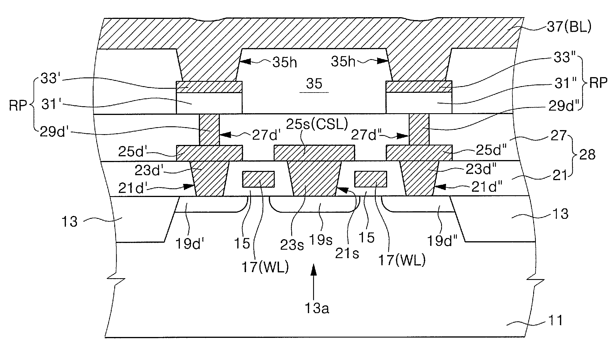
[0033]The present invention will now be described more fully hereinafter with reference to the accompanying drawings, in which preferred embodiments of the invention are shown. This invention may, however, be embodied in different forms and should not be construed as limited to the embodiments set forth herein. Rather, these embodiments are provided so that this disclosure will be thorough and complete, and will fully convey the scope of the invention to those skilled in the art. In the drawings, the thickness of layers and regions are exaggerated for clarity. Like numbers refer to like elements throughout the specification.

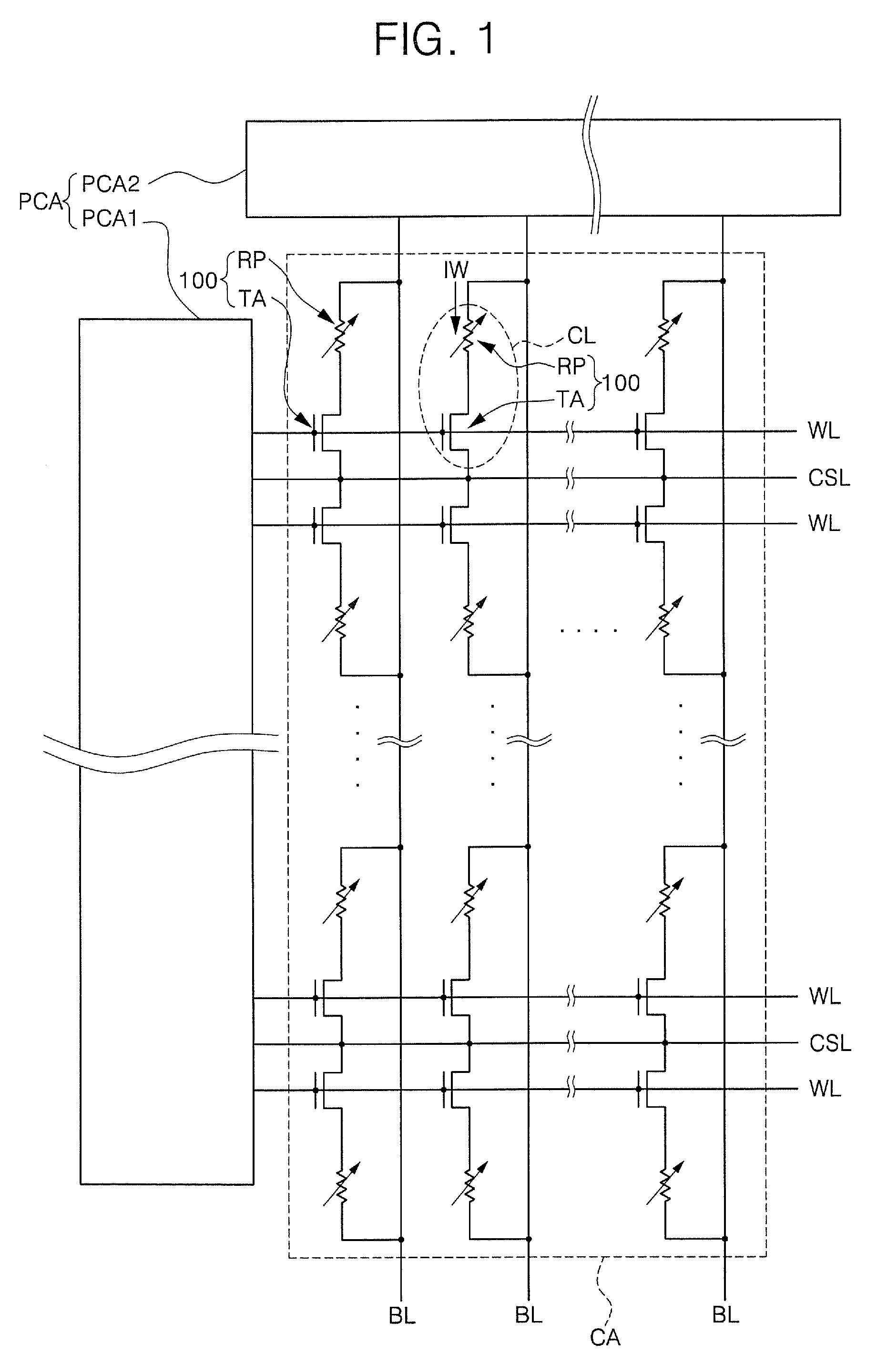
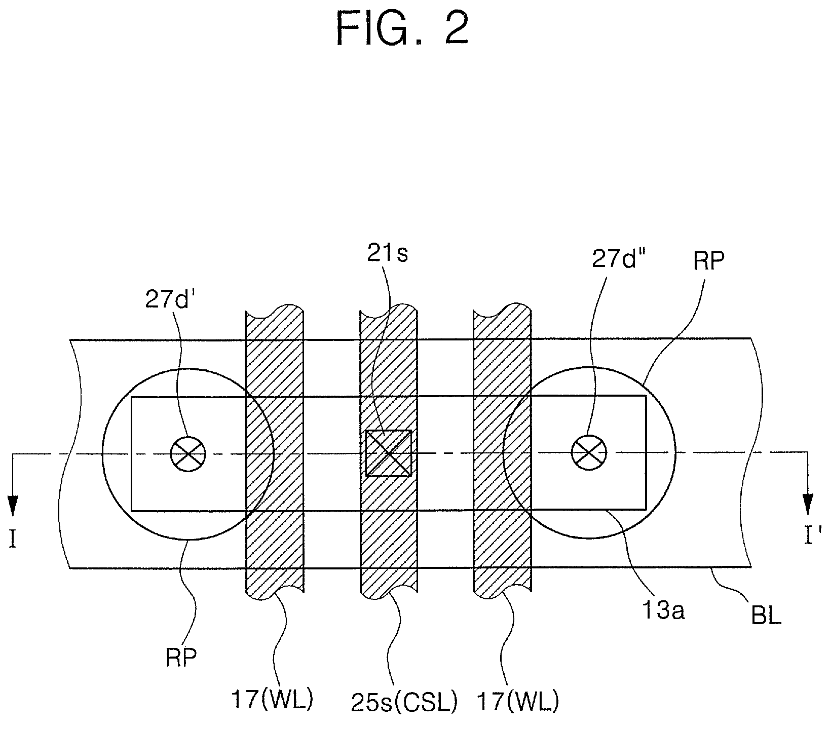
[0034]FIG. 1 is a schematic block diagram of a phase change memory device employing phase change memory cells according to an exemplary embodiment of the present invention. Referring to FIG. 1, the phase change memory device includes a cell array area CA and a peripheral circuit area PCA. The cell array area CA (i.e., a memory cell region) includes a plurality of...


PUM


Abstract

A phase change memory cell includes an interlayer insulating layer formed on a semiconductor substrate, and a first electrode and a second electrode disposed in the interlayer insulating layer. A phase change material layer is disposed between the first and second electrodes. The phase change material layer may be an undoped GeBiTe layer, a doped GeBiTe layer containing an impurity or a doped GeTe layer containing an impurity. The undoped GeBiTe layer has a composition ratio within a range surrounded by four points (A1(Ge21.43, Bi16.67, Te61.9), A2(Ge44.51, Bi0.35, Te55.14), A3(Ge59.33, Bi0.5, Te40.17) and A4(Ge38.71, Bi16.13, Te45.16)) represented by coordinates on a triangular composition diagram having vertices of germanium (Ge), bismuth (Bi) and tellurium (Te). The doped GeBiTe layer contains an impurity and has a composition ratio within a range surrounded by four points (D1(Ge10, Bi20, Te70), D2(Ge30, Bi0, Te70), D3(Ge70, Bi0, Te30) and D4(Ge50, Bi20, Te30)) represented by coordinates on the triangular composition diagram.

Description

REFERENCE TO PRIORITY APPLICATION[0001]This application claims priority to Korean Patent Application No. 2006-45298, filed May 19, 2006, the disclosure of which is hereby incorporated herein by reference.FIELD OF THE INVENTION[0002]The present invention relates to nonvolatile memory devices, and more particularly, to a phase change memory cell employing a GeBiTe layer as a phase change material layer, a phase change memory device including the same, an electronic system including the same, and a method of fabricating the same.BACKGROUND OF THE INVENTION[0003]Nonvolatile memory devices retain their stored data even when their power supplies are turned off. Thus, the nonvolatile memory devices are widely used in computers, mobile telecommunication systems, memory cards and so on.[0004]Recently, other types of nonvolatile memory devices, for example, phase change memory devices are being used. A unit cell of a phase change memory device includes a switching device and a data storage el...

Claims


Application Information

Patent Timeline
Patent Type & Authority Patents(United States)
IPC IPC(8): G11C11/00
CPCG11C11/5678G11C13/0004H01L27/2409H01L27/2436H01L27/2463H01L45/06H01L45/1233H01L45/144H01L45/1625G11C2213/72G11C2213/79H10B63/20H10B63/30H10B63/80H10N70/231H10N70/826H10N70/8828H10N70/026
Inventor KUH, BONG-JINHA, YONG-HOPARK, DOO-HWANPARK, JEONG-HEEKO, HAN-BONG
Owner SAMSUNG ELECTRONICS CO LTD
Why Eureka
Try Eureka