Glass substrate having circuit pattern and process for producing the same

a glass substrate and circuit technology, applied in the field of glass substrates with circuit patterns, can solve the problems of high production costs, low yield, and high production costs, and achieve the effects of reducing or scattering of visible light transmittance, small masks, and increasing strain stress

Inactive Publication Date: 2010-12-07
ASAHI GLASS CO LTD
View PDF11 Cites 2 Cited by
  • Summary
  • Abstract
  • Description
  • Claims
  • Application Information

AI Technical Summary

Benefits of technology

[0042]According to the invention, a laser irradiation defect formed by laser patterning such as stepwise irradiation can be dissipated by a simple method, and as a result, a glass substrate having a circuit pattern which is free from a laser irradiation defect can be provided. Also, a reduction or scattering of visible light transmittance of the glass substrate having a circuit pattern, an increase of strain stress and the like are not generated.
[0043]Also, it is possible to achieve micro patterning so that a circuit with higher integration (higher definition) can be formed, and a small mask can be used. Therefore, the invention is excellent in view of costs and is able to suppress the production costs through minimization of the number of steps. Also, a large amount of a liquid developer, a chemical liquid such as an etching agent and a rinsing liquid are not used; and the production costs and environmental loads can be suppressed; and patterning using a material which has hitherto been hardly applied for etching with an etching agent or the like can be achieved. Furthermore, it is possible to provide a process for producing a glass substrate having a circuit pattern which is free from the generation of a laser irradiation defect.

Problems solved by technology

For that reason, there was involved a problem that the production costs are very high.
This involved a problem that not only the yield is low, and the production costs are very high, but environmental loads such as a liquid-waste treatment which has become recently a matter of concern are very large.
Furthermore, etching with an etching agent, etc. was difficult depending upon the kind of a material to be used for a metal oxide film or the like.
In consequence, only limited materials having excellent etching properties could be applied in the photolithography etching process.
Such a laser irradiation defect reduces the quality of the glass substrate having a circuit pattern.
For example, when this is used as a glass substrate for plasma display, a visible light transmittance of the laser irradiation defective portion differs from that in other portions, thereby adversely influencing the display of a screen.

Method used


Image

  • Glass substrate having circuit pattern and process for producing the same
  • Glass substrate having circuit pattern and process for producing the same
  • Glass substrate having circuit pattern and process for producing the same

Examples


example 1

[0161]A glass substrate (PD200, manufactured by Asahi Glass Co., Ltd.) of 40 mm in square and 2.8 mm in thickness was prepared. This glass substrate has an average coefficient of linear expansion at from 50 to 350° C. (JIS-R3102 (1995)) of 83×10−7 / ° C., a strain point (JIS-R3104 (1995)) of 570° C. and a softening point (JIS-R3103 (1995)) of 830° C.

[0162]This glass substrate is also hereinafter referred to as “glass substrate A”.

[0163]An antimony-doped tin oxide film was formed on one principal surface of this glass substrate A using a sputtering fabrication apparatus.

[0164]Specifically, the sputtering fabrication was carried out using, as a target, a sintered body containing 95% by mass of tin oxide and 5% by mass of antimony oxide at an initial degree of vacuum of 1.3×10⁻⁴ Pa, a glass sheet temperature of 250° C. and a degree of vacuum at the time of introduction of an argon / oxygen gas of 6.7×10⁻¹ Pa (at that time, an oxygen partial pressure was 5%).

[0165]As a result, a 300 nm-thic...

example 2

[0189]Tests were carried out under the same operations and conditions and the like as in Example 1, except for using a low-melting point glass having a softening point of 620° C. in place of the low-melting point glass having a softening point of 478° C. as used in Example 1.

[0190]Then, a cross-section of the glass substrate having a low-melting point glass formed thereon was observed by an optical microscope and an electronic microscope. As a result, the low-melting point glass had a thickness of 20 μm. Also, the compatible layer had a thickness of 0.15 μm, and it was confirmed that a laser irradiation defect was dissipated.

[0191]While the invention has been described in detail and with reference to specific embodiments thereof, it will be apparent to one skilled in the art that various changes and modifications can be made therein without departing from the spirit and scope thereof.

[0192]This application is based on Japanese Patent Application No. 2005-366410 filed Dec. 20, 2005, ...


PUM

PropertyMeasurementUnit
softening pointaaaaaaaaaa
melting pointaaaaaaaaaa
temperatureaaaaaaaaaa

Abstract

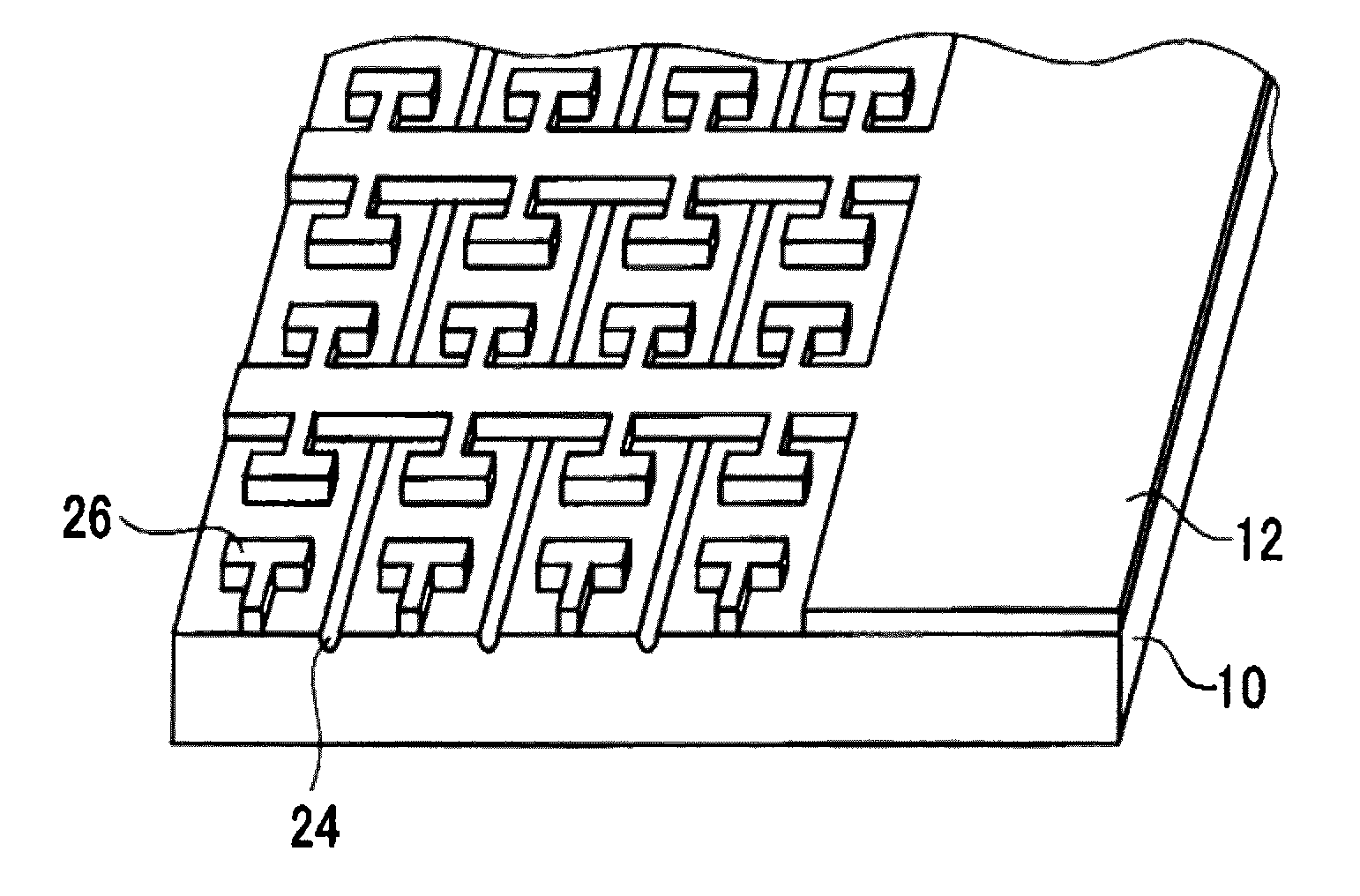
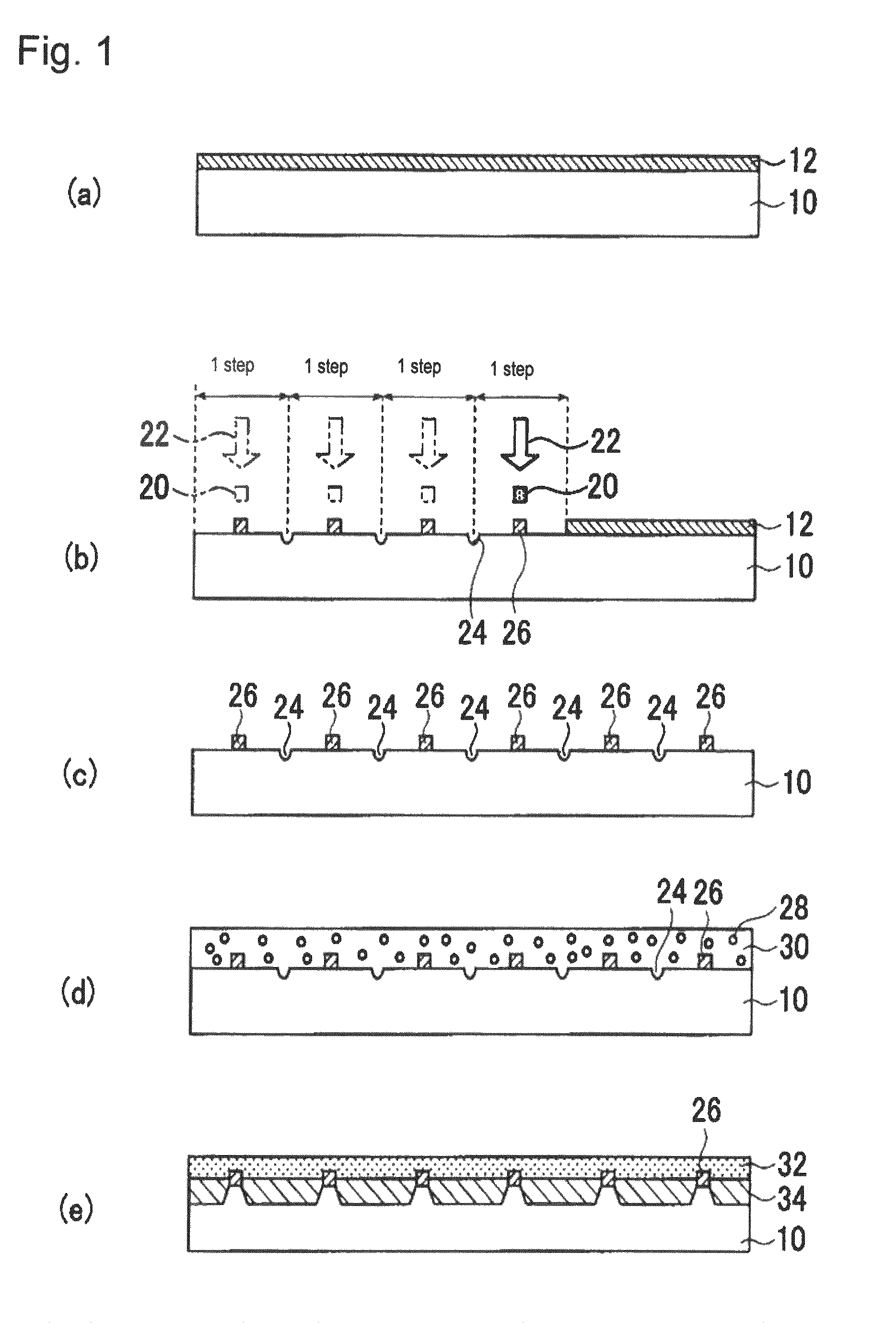
A process for producing a glass substrate having a circuit pattern is disclosed. The process includes forming a thin film layer on a glass substrate and then irradiating the thin film layer with laser light to form a circuit pattern on the glass substrate; depositing a low-melting point glass having a softening point of from 450 to 630° C. on the glass substrate having the circuit pattern formed thereon; and sintering the low-melting point glass to form a low-melting point glass layer which includes the low-melting point glass sintered on the glass substrate having the circuit pattern formed thereon and which forms a compatible layer between the glass substrate and the low-melting point glass layer.

Description

TECHNICAL FIELD[0001]The present invention relates to a glass substrate having a circuit pattern and a process for producing the same.BACKGROUND ART[0002]An electronic circuit board having a circuit pattern comprising a metal or an insulating material in a thin film form on a substrate has hitherto been used for computers, communications, information home appliances, various display devices and the like.[0003]Then, in order to respond to the rapidly developing high-level information society, this electronic circuit board is required to realize higher integration (higher definition) and larger area.[0004]For forming this circuit pattern, there has been generally employed a method using a photolithography etching process. A typical process of this method is illustrated in FIGS. 9 and 10.[0005]Here, FIG. 9 illustrates a part of conventional steps of forming a circuit pattern, in which (a) to (e) are each a cross-sectional view illustrating a diagrammatic configuration of an electronic ...

Claims


Application Information

Patent Timeline
Patent Type & Authority Patents(United States)
IPC IPC(8): G03F7/26G03F7/20H01J9/02H01J11/22H01J11/24H01J11/34H05K3/08H05K3/28
CPCH01J9/02H01J11/12H01J11/34H05K3/28H05K1/0306Y10T428/24868H05K3/38H05K2201/0269H05K3/027H05K3/04
Inventor SATOH, RYOHEINAKAGAWA, KOJIUSUI, REOTANAKA, KENJITAKAKI, SATORUEBATA, KENICHIAOKI, YUMIKO
Owner ASAHI GLASS CO LTD
Why Eureka
Try Eureka