

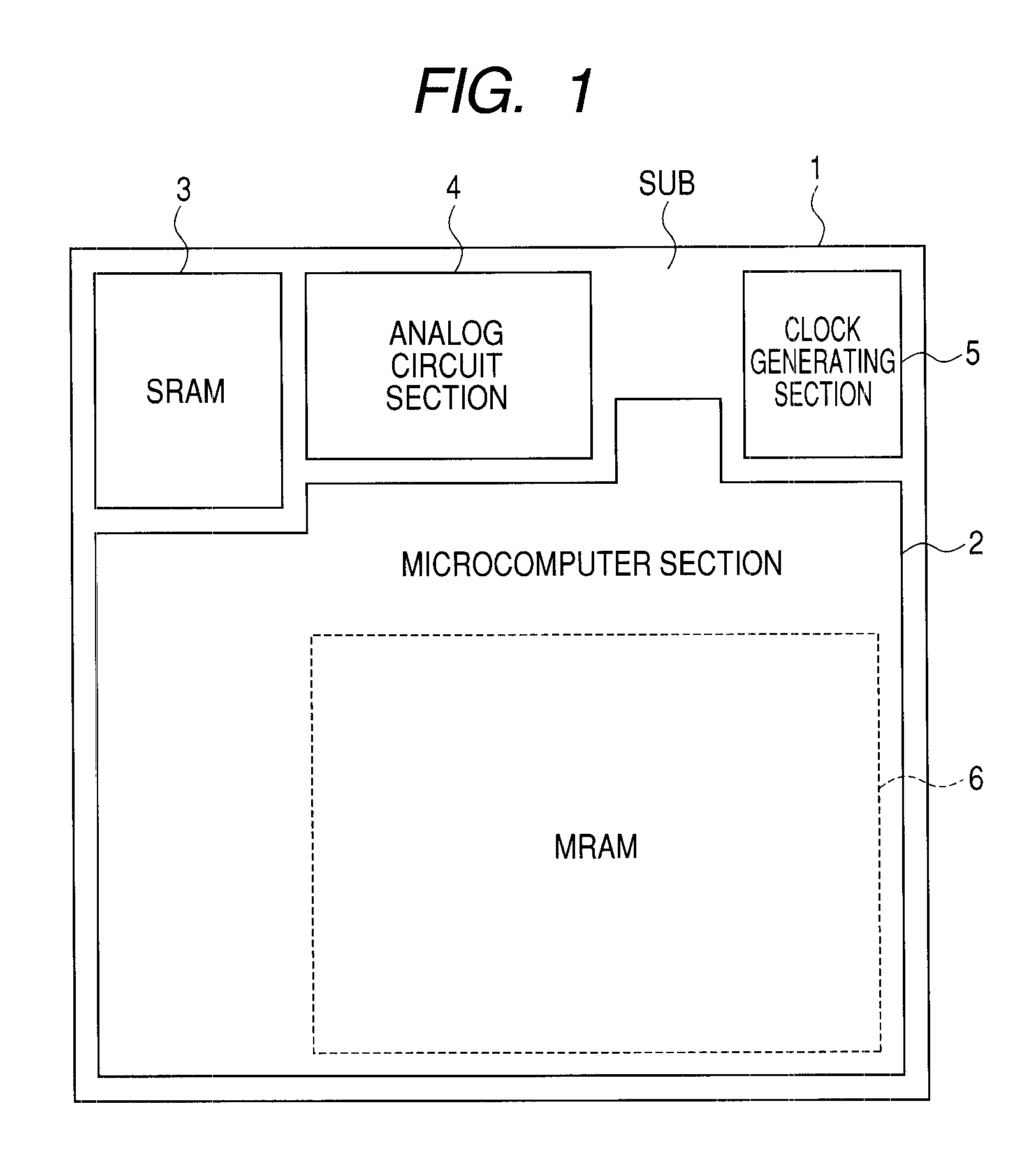
Semiconductor device
a technology of semiconductor devices and dielectric capacitors, applied in semiconductor devices, digital storage, instruments, etc., can solve the problems of difficult to ensure compatibility between the enhancement of data read speed and the reduction of circuit area, and the signal transmission delay of data read, so as to enhance data read speed, reduce the number of word line drive circuits, and speed up the effect of speed
- Summary
- Abstract
- Description
- Claims
- Application Information
AI Technical Summary
Benefits of technology
Problems solved by technology
Method used
Image

Examples
first embodiment
Modification of First Embodiment
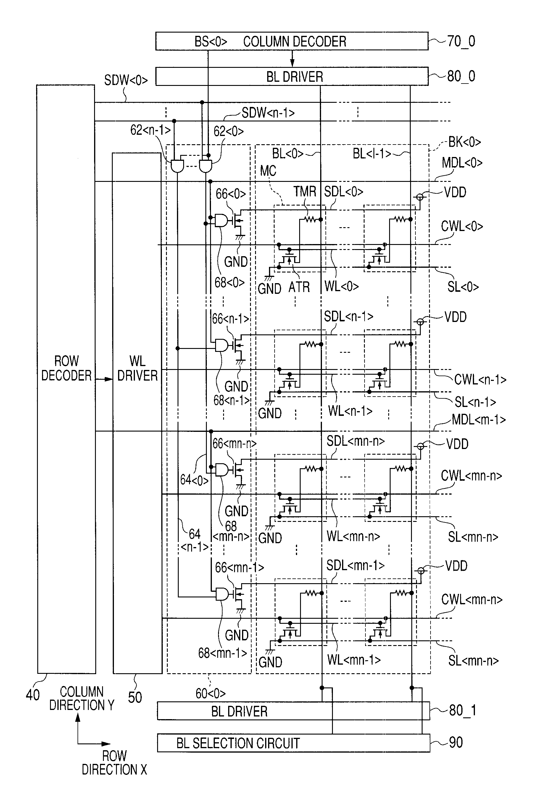
[0124]By modifying the shapes and arrangements of constituent elements in the memory array according to claim 1, it is possible to further enhance the integration density of the memory array. In this modification, the structure from the semiconductor substrate to the second metal wiring layer M2 in the sectional view of FIG. 8 is modified. More specifically, there are performed (i) interconnection of the source regions of memory cells, (ii) change of the wiring of the source line, and (iii) change of the shape and arrangement of the connection portion between the word line and the common word line. Hereinafter, detailed description will be made with reference to FIGS. 9 to 11. The connection portion is also called a common portion or a shunt portion.
[0125]FIG. 9 is a plan view showing the pattern layout of a memory array according to a modification of the first embodiment.
[0126]FIG. 10 is a sectional view taken along line X-X of FIG. 9. FIGS. 9 and 10...
second embodiment
Modification of Second Embodiment
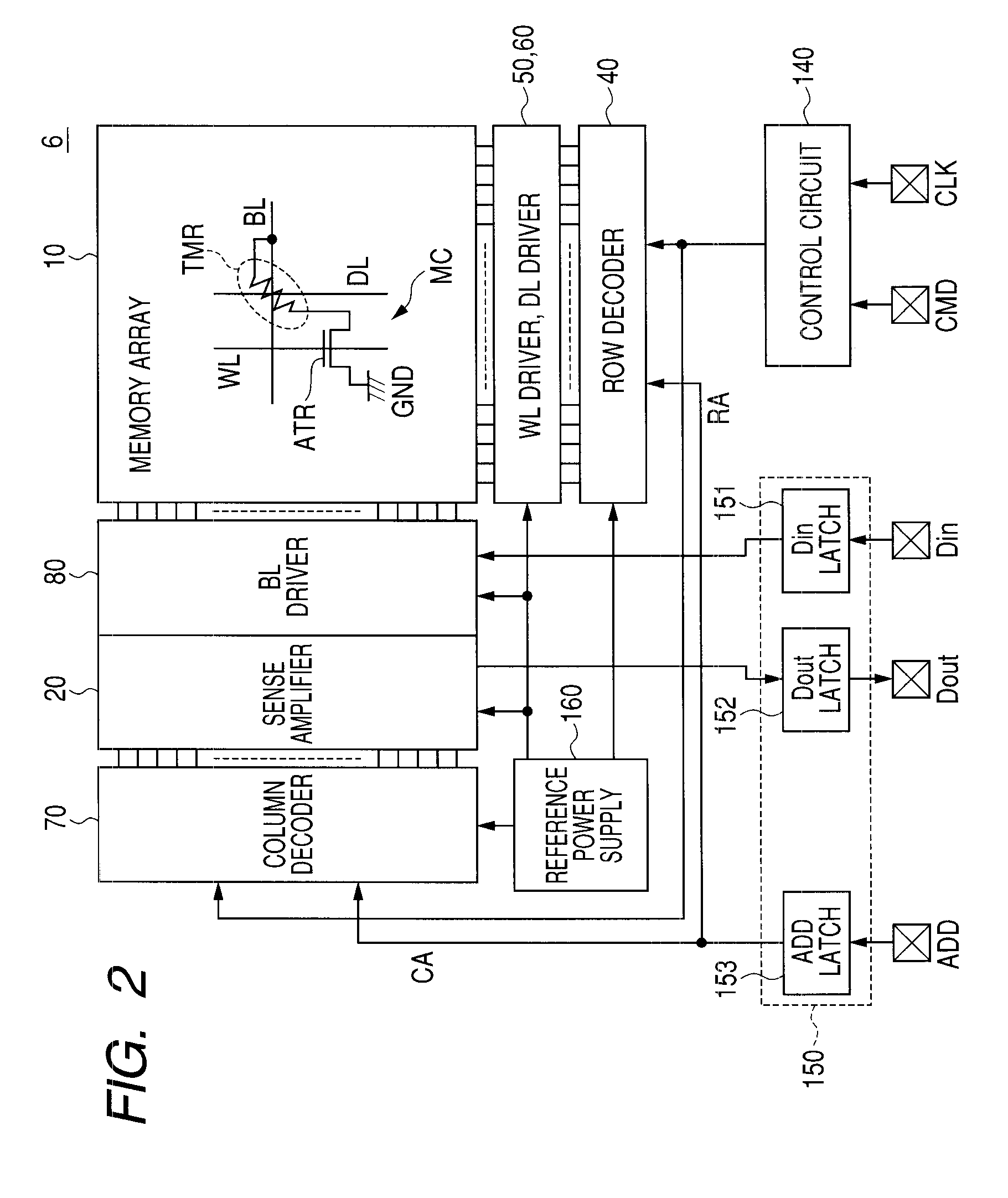
[0199]There are cases where a power supply voltage to the drive circuit of the digit line DL is set to be higher than a power supply voltage to the drive circuit of the word line WL in order to ensure a necessary and sufficient write current. Such a plurality of internal voltages are required, for example, to reduce the power consumption of the entire MRAM section.
[0200]More specifically, the power supply voltage coupled to the sub-digit line SDL in FIG. 13 is increased to VDD2. Further, in order to increase the gate drive voltage of the drive transistor 66 in the digit line driver 60, the power supply voltage for driving the AND gate 68 is increased to VDD2, and the voltage level of an input signal to the AND gate 68 is increased. Accordingly, in a modification of the second embodiment, the H-level voltage of a main decode signal is increased to VDD2 by a level shifter 45 provided in a row decoder 40B before the main decode signal is outputted to th...
third embodiment
[0213]In the MRAM section 6 according to the first embodiment, by disposing the common word line CWL, it is possible to read data at high speed and reduce the area of the circuit for row selection. However, from the viewpoint of the memory cell structure, the MRAM section 6 according to the first embodiment requires a metal wiring layer for the common word line CWL, which leads to the five metal wiring layers in total.
[0214]In the MRAM section 6 according to the third embodiment, the digit line driver 60 transmits a row selection signal during data write through the common word line CWL. This negates the need for the main digit line MDL; accordingly, it is possible to reduce one metal wiring layer in the MRAM section 6 according to the first embodiment. Further, a latch circuit 92 is disposed to hold the active state of the common word line CWL, thereby making a contrivance of providing a lag between timing for activating the common word line CWL and timing for supplying a current t...
PUM
 Abstract
Description
Claims
Application Information