Photoelectric conversion device and method for manufacturing the same

a technology photoelectric conversion method, which is applied in the direction of semiconductor device, coating, plasma technique, etc., can solve the problems of low penetration rate of photoelectric conversion device using amorphous silicon thin film, inability to overcome, and lower photoelectric conversion efficiency than that of bulk photoelectric conversion device, etc., to achieve high productivity, improve photoelectric conversion characteristics, and low cost

Inactive Publication Date: 2011-02-15
SEMICON ENERGY LAB CO LTD
View PDF14 Cites 13 Cited by
  • Summary
  • Abstract
  • Description
  • Claims
  • Application Information

AI Technical Summary

Benefits of technology

[0012]Alternatively, a semiconductor source gas and a dilution gas which are mixed in a mixing ratio at which a microcrystalline semiconductor can be formed are introduced into a reaction space and plasma is produced to deposit a film. Thus, a microcrystalline semiconductor layer is formed. A film is deposited on the microcrystalline semiconductor layer by reducing the flow ratio of a dilution gas to a semiconductor source gas as compared to a reaction gas used for deposition of the microcrystalline semiconductor layer. Thus, an amorphous semiconductor layer including a crystal with a three-dimensional shape tapered in a direction of deposition of the film (a needle-like crystal) is formed over the microcrystalline semiconductor layer.
[0016]Another embodiment of the present invention is a method for manufacturing a photoelectric conversion device including the steps of forming a first electrode over a substrate; forming a first semiconductor layer of a microcrystalline semiconductor including an impurity element imparting one conductivity type, over the first electrode, by introducing a reaction gas including a semiconductor source gas and a dilution gas which are mixed in a mixing ratio at which a microcrystalline semiconductor can be formed into a reaction chamber and producing plasma to deposit a film; forming a second semiconductor layer including a crystal with a three-dimensional shape tapered in a direction of deposition of a film, over the first semiconductor layer, by reducing a flow ratio of the dilution gas to the semiconductor source gas as compared to the reaction gas used for the first semiconductor layer to deposit the film; forming a third semiconductor layer including an impurity element imparting a conductivity type opposite to the first semiconductor layer, over the second semiconductor layer; and forming a second electrode over the third semiconductor layer.
[0020]According to one embodiment of the present invention, an amorphous semiconductor layer having a needle-like crystal is formed as a layer which converts light into electricity, whereby photoelectric conversion characteristics can be improved. Further, an amorphous semiconductor layer is deposited on a microcrystalline semiconductor layer by controlling the amount of dilution of a reaction gas, whereby a crystal with a three-dimensional tapered shape can be made to grow. In addition, a main portion which converts light into electricity is formed using an amorphous semiconductor layer; therefore, high productivity and low cost can be achieved and resources can be saved. Thus, a photoelectric conversion device with improved cost competitiveness can be provided.

Problems solved by technology

However, the penetration rate of photoelectric conversion devices using amorphous silicon thin films is lower than that of bulk photoelectric conversion devices because problems of photodegradation called Staebler-Wronski effect, lower photoelectric conversion efficiency than that of a bulk photoelectric conversion device, or the like can not be overcome.

Method used


Image

  • Photoelectric conversion device and method for manufacturing the same
  • Photoelectric conversion device and method for manufacturing the same
  • Photoelectric conversion device and method for manufacturing the same

Examples


embodiment 1

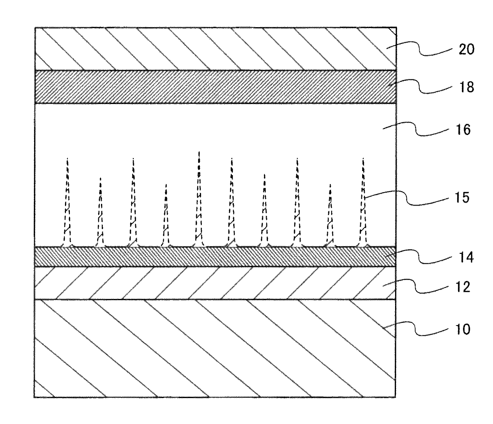
[0044]FIG. 1 shows a structure of a photoelectric conversion device according to this embodiment. A photoelectric conversion device shown in FIG. 1 has a structure including a first electrode 12 provided over a substrate 10, a first semiconductor layer 14 provided over the first electrode 12, a second semiconductor layer 16 provided over the first semiconductor layer 14, a third semiconductor layer 18 provided over the second semiconductor layer 16, and a second electrode 20 provided over the third semiconductor layer 18. The second semiconductor layer 16 is interposed between the first semiconductor layer 14 and the third semiconductor layer 18. The first semiconductor layer 14 and the third semiconductor layer 18 have opposite polarities. One of the first semiconductor layer 14 and the third semiconductor layer 18 is formed using a p type semiconductor, and the other is formed using an n type semiconductor. The second semiconductor layer 16 is formed using an i type semiconductor....

embodiment 2

[0075]In this embodiment, an example of a so-called integrated photoelectric conversion device is described, in which a plurality of unit cells is formed over one substrate and is connected in series to integrate a photoelectric conversion device. Hereinafter, a manufacturing process and a structure of an integrated photoelectric conversion device are described.

[0076]In FIG. 5A, a first electrode layer 102 is provided over a substrate 101. Alternatively, a substrate 101 provided with a first electrode layer 102 is prepared. The first electrode layer 102 is formed to a thickness of 40 nm to 200 nm (preferably, 50 nm to 100 nm) using a transparent conductive material such as indium oxide, an indium tin oxide alloy, zinc oxide, tin oxide, or indium tin oxide-zinc oxide alloy. The sheet resistance of the first electrode layer 102 may be about 20 Ω / square to 200 Ω / square.

[0077]The first electrode layer 102 can be formed using a conductive high molecular material (also referred to as a co...

embodiment 3

[0122]In this embodiment, an example of a photo-sensor device is described as another mode of a photoelectric conversion device.

[0123]FIG. 9 shows an example of a photo-sensor device according to this embodiment. This photo-sensor device shown in FIG. 9 has a photoelectric conversion layer 225 in a light receiving portion and a function of amplifying an output from the photoelectric conversion layer 225 and outputting the output by an amplifier circuit including a thin film transistor 211. The photoelectric conversion layer 225 and the thin film transistor 211 are provided over a substrate 201. As the substrate 201, a substrate having a light-transmitting property, such as a glass substrate, a quartz substrate, or a ceramic substrate can be used.

[0124]An insulating layer 202 including one or more of silicon oxide, silicon nitride oxide, silicon nitride, and silicon oxynitride is provided over the substrate 201 by a sputtering method or a plasma CVD method. The insulating layer 202 i...


PUM


Abstract

To provide a photoelectric conversion device with improved photoelectric conversion characteristics and cost competitiveness. A photoelectric conversion device including a semiconductor junction has a semiconductor layer in which a needle-like crystal is made to grow over an impurity semiconductor layer. The impurity semiconductor layer is formed of a microcrystalline semiconductor and includes an impurity imparting one conductivity type. An amorphous semiconductor layer is deposited on a microcrystalline semiconductor layer by setting the flow rate of a dilution gas (typically silane) to 1 time to 6 times the flow rate of a semiconductor source gas (typically hydrogen) at the time of deposition. Thus, a crystal with a three-dimensional shape tapered in a direction of the deposition of a film, i.e., in a direction from the microcrystalline semiconductor layer to the amorphous semiconductor layer is made to grow.

Description

BACKGROUND OF THE INVENTION[0001]1. Field of the Invention[0002]The present invention relates to a photoelectric conversion device having a semiconductor junction and a method for manufacturing the photoelectric conversion device.[0003]2. Description of the Related Art[0004]In response to global environmental issues in recent years, the market for photoelectric conversion devices typified by solar cells such as residential photovoltaic systems has expanded. Bulk photoelectric conversion devices which are formed using single crystal silicon or polycrystalline silicon with high photoelectric conversion efficiency have already been put into practical use. The photoelectric conversion devices using single crystal silicon or polycrystalline silicon are manufactured by being cut out of large silicon ingots. However, it takes a long time to manufacture large silicon ingots, which means productivity is low, and since supply of raw materials of silicon itself is limited, the supply of silico...

Claims


Application Information

Patent Timeline
Patent Type & Authority Patents(United States)
IPC IPC(8): H01L21/00
CPCH01L31/03685H01L31/03762H01L31/1816Y02E10/545Y02E10/548
Inventor YAMAZAKI, SHUNPEITORIUMI, SATOSHIYOKOI, TOMOKAZUFURUNO, MAKOTO
Owner SEMICON ENERGY LAB CO LTD
Why Eureka
Try Eureka