Fin field effect transistor having low leakage current and method of manufacturing the FinFET

a technology of field effect transistor and finfet, which is applied in the direction of transistors, electrical devices, semiconductor devices, etc., can solve the problems of inability to relatively shorten the depth of source/drain, drain current increase in an off state, and reduce the size of cell devices, etc., to achieve low leakage current

Active Publication Date: 2011-03-15
SEOUL NAT UNIV R&DB FOUND
View PDF4 Cites 29 Cited by
  • Summary
  • Abstract
  • Description
  • Claims
  • Application Information

AI Technical Summary

Benefits of technology

[0049]FIG. 15 is a graph illustrating ID-VGS characteristics of a device according to changes in a length of the second gate electrode having a low work function in the structure of the FinFET having low leakage current illustrated in FIG. 14 according to the present invention. Referring to FIG. 15, the total gate length is 50 nm, a width d1 of the fence-shaped body is 20 nm, a side channel height d2 of the fence-shaped body is 50 nm, a substrate density is p-type 1017 cm−3, a thickness of the gate oxide layer is 3 nm, and a drain voltage is 1.5V. In addition, p-type impurities having a peak value of 31018 cm−3 are doped in a Gaussian function form rather below the distance d2 from the upper portion of the fence-shaped body to solve punchthrough between the source and the drain which may occur at a position lower than the upper portion of the fence-shaped body by the distance d2. As illustrated in FIG. 15, a length of the n+ region having a low work function is changed from 0 to 50 nm to examine characteristics thereof. The n+ region having a length of 0 means that the gate only includes the p+ gate, and the n+ region having a length of 50 nm means that the gate only includes the n+ gate. At a region where the drain current A is 10−13 or less, due to GIDL, the drain current increases as a gate voltage is changed from positive to negative. As an important characteristic of the DRAM cell device, current in a case where the gate voltage VGS is 0V and the drain voltage is the maximum voltage in operating voltages is called Ioff. As illustrated in results of FIG. 15, when the length of the gate electrode having a low work function is changed, a value thereof is also changed.
[0050]FIG. 16 is a graph illustrating the Ioff current for the device described with reference to FIG. 15 according to an n+ gate length. Structures and bias conditions of all devices are the same as those in FIG. 15. As illustrated in FIG. 16, the Ioff current has the minimum value when the n+ gate length in the gate electrode having the total length of 50 nm is about 15 nm. As described above, when the gate structure according to the present invention is used, the Ioff current due to GIDL in the bulk FinFET having a high density can be reduced, so that the bulk FinFET can be used as the DRAM cell device having a gate length of 50 nm or less.

Problems solved by technology

Reduction of the size of the cell device has a problem of the short channel effect.
Due to the short channel effect, there is a problem in that drain current increases in an OFF state.
In addition, a depth of the source / drain cannot be relatively shortened, and this is an obstacle to reduce the size of the cell device.
In this case, an electric field between the channel and the drain increases, and leakage current increases due to band-to-band tunneling.
Therefore, it is expected that reducing the gate length of the cell device of the MOSFET having the conventional flat channel to be about 70 nm or less is very difficult.
However, there is a problem in that the on-current is significantly reduced due to a relatively long channel length and a narrow channel width.
The reduction of the on-current may cause reduction of an operating speed of the DRAM.
In addition, the recessed channel region may have two corners in a direction of the channel length, and when the channel doping density is changed at the corners, there is a problem in that the threshold voltage is significantly changed.
However, in this case, the doping density affects the corner area.
There is a worse problem in that when the recessed channel width is reduced as the size of the device is reduced, an etching profile adjacent to the recessed bottom cannot be easily controlled, and it is difficult to uniformly control the recessed channel depth.
Since the structure of the channel of the recessed channel device is concave, back-bias effects heavily occur.
In addition, for negative substrate bias, an n-channel MOSFET (NMOS) has a problem in that a threshold voltage is significantly increased as compared with the flat channel.
However, it is impossible to apply the double / triple-gate device implemented on a silicon on insulator (SOI) (referred to as SOI FinFET) as the DRAM cell device due to device characteristics.
However, when an n+ polycrystalline silicon gate is applied to a conventional n-type FinFET, a threshold voltage of the device is low, so that there is a disadvantage in that current in the OFF state increases.
When a channel doping density is increased in order to increase the threshold voltage, leakage current due to band-to-band tunneling between a drain and the channel is increased, so that increasing the channel doping density is not effective.
However, in this case, there are problems in that the negative wordline method is not general and peripheral circuits become complex.
However, in this case, band bending increases at a drain region which overlaps with a gate electrode, so that there are problems in that GIDL is increased, and off-current is increased.
When an SOI substrate is used to implement the FinFET, there are disadvantages in that the SOI substrate has more defects and more expensive than the bulk silicon substrate.
The FinFET implemented on the SOI substrate has a floating body problem that is the problem of the conventional SOI device.
In addition, in the FinFET implemented on the SOI substrate, leakage current may increase due to the defects, so that the FinFET implemented on the SOI may not be applied to the DRAM which is sensitive to leakage current.
However, in this case, there is a problem in that GIDL per channel width increases at a given surface, and this results in decrease of a refresh time of the DRAM cell.
In this structure, there is a disadvantage in that the side gate 8 is formed in a spacer shape and a practical gate length is increased.
Particularly, the SOI device structure is not appropriate to be applied to a device that is sensitive to leakage current such as the DRAM.
Since a channel structure is a flat channel structure, the channel structure has problems of the conventional flat channel structure.
However, the structure is formed on the SOI substrate, the structure has problems of the SOI device.
In addition, the side gate having a low work function of the upper gate is electrically isolated from the main gate having a high work function, so that there is a problem in that an area of the device is increased in the device manufacturing process.

Method used


Image

  • Fin field effect transistor having low leakage current and method of manufacturing the FinFET
  • Fin field effect transistor having low leakage current and method of manufacturing the FinFET
  • Fin field effect transistor having low leakage current and method of manufacturing the FinFET

Examples


second embodiment

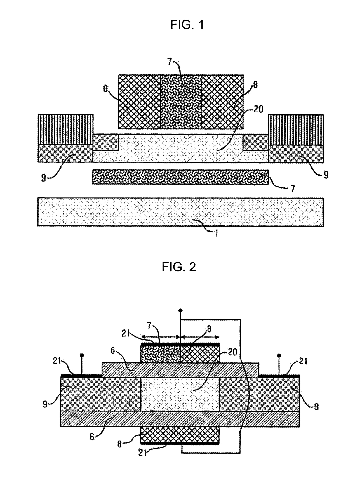
[0101]Hereinafter, a FinFET having low leakage current according to a second embodiment of the present invention will be described in detail. FIG. 8a is a perspective view illustrating the FinFET according to the second embodiment of the present invention, and FIG. 8b is a cross-sectional view taken along line A-A′ of FIG. 8a. Referring to FIG. 8, the FinFET according to the second embodiment includes a substrate 810, a fence-shaped body 820, a gate insulating layer 830, a first insulating layer 832, a nitride layer 840, a second insulating layer 850, a first gate electrode 870, a second gate electrode 880, and source / drain regions 890 and 892. A description of components of the FinFET according to the second embodiment that are the same as those according to the first embodiment is omitted for the convenience of description.

[0102]The second insulating layer 850 is a device isolating layer for electrically isolating a corresponding device from an adjacent device and is also called a...

third embodiment

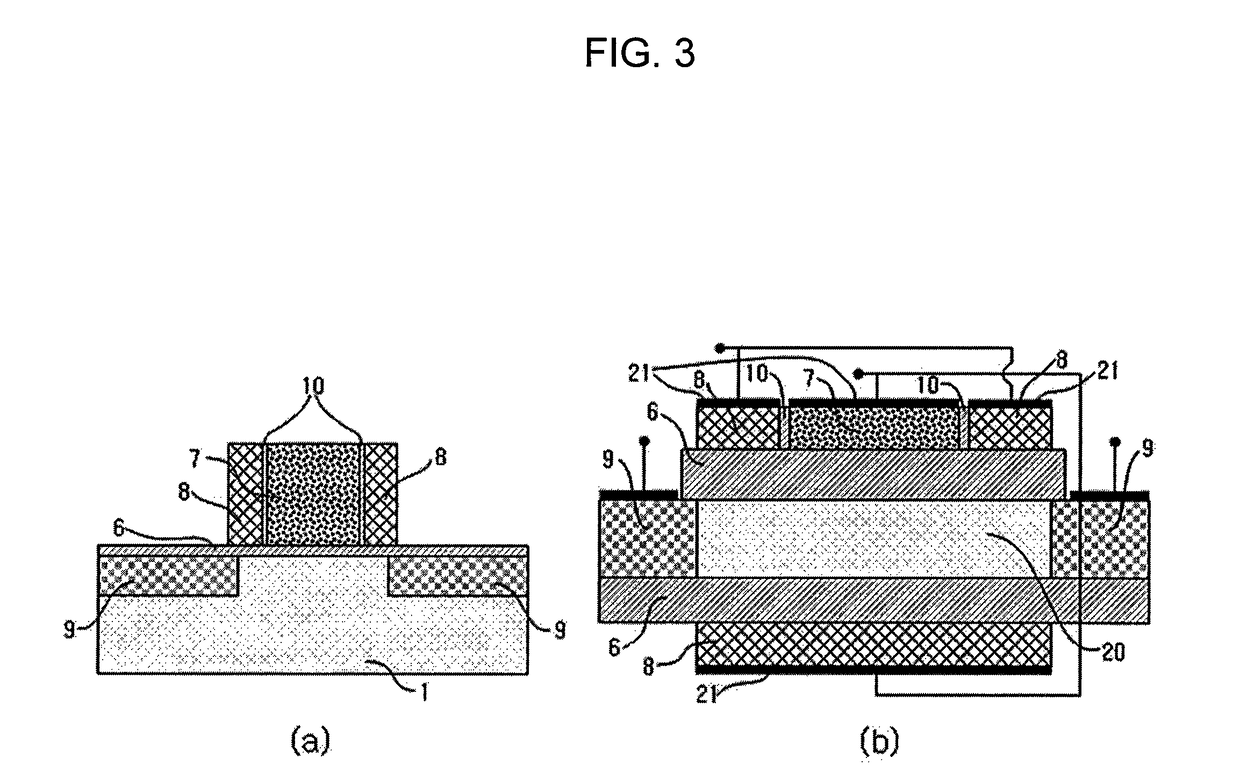
[0106]Hereinafter, a structure of a FinFET having low leakage current according to a third embodiment of the present invention will be described in detail with reference to FIG. 10. Components of the FinFET according to the current embodiment excluding a gate electrode are the same as those according to the first embodiment, so that a detailed description thereof is omitted.

[0107]FIG. 10a is a perspective view and FIG. 10b is a top plan view illustrating the FinFET 101 according to the third embodiment of the present invention. Referring to FIG. 10, the FinFET according to the third embodiment of the present invention includes second gate electrodes 1080 and 1082 having low work functions disposed at both side surfaces of a first gate electrode 1070 having a high work function. In the aforementioned structure of the gate electrode, a drain region and a source region overlap with the second gate electrodes 1080 and 1082 having low work functions. Accordingly, GIDL can be reduced. How...

fourth embodiment

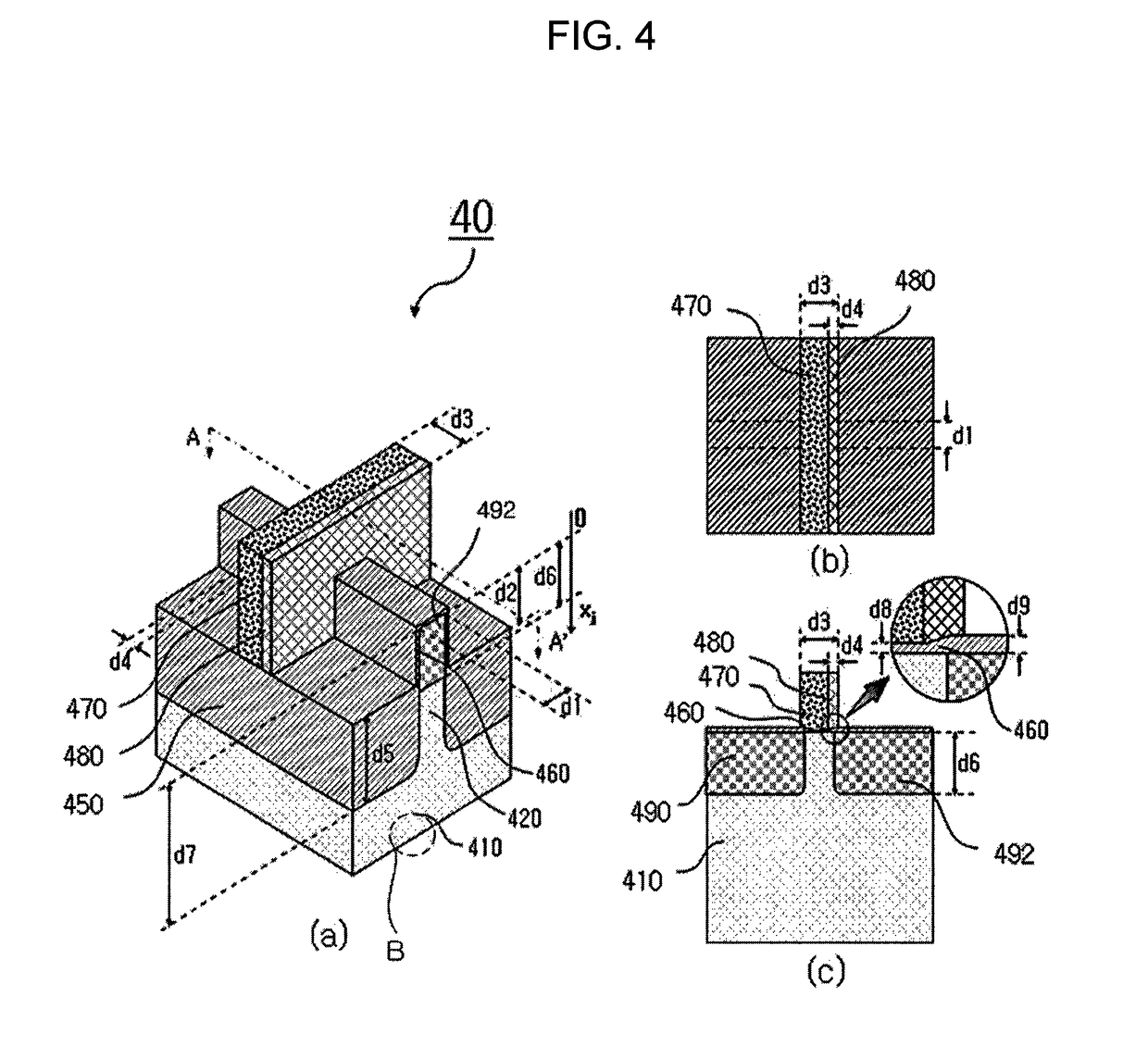
[0109]Hereinafter, a structure of a FinFET 111 having low leakage current according to a fourth embodiment of the present invention will be described in detail with reference to FIG. 11. Components of the FinFET according to the current embodiment excluding a gate electrode are the same as those according to the first embodiment, so that a detailed description thereof is omitted.

[0110]FIG. 11a is a perspective view and FIG. 11b is a top plan view illustrating the FinFET according to the fourth embodiment of the present invention. Referring to FIG. 11, the FinFET according to the fourth embodiment of the present invention further includes an isolation insulating layer 1182 for electric isolation provided between a first gate electrode 1170 having a high work function and a second gate electrode 1180 having a low work function. A thickness d12 of the added isolation insulating layer 1182 ranges from 0.5 to 10 nm.

[0111]The structure of the gate electrode according to the fourth embodim...


PUM


Abstract

Provided is a fin field effect transistor (FinFET) having low leakage current and a method of manufacturing the same. The FinFET includes: a bulk silicon substrate; a fence-shaped body formed by patterning the substrate; an insulating layer formed on a surface of the substrate to a first height of the fence-shaped body; a gate insulating layer formed at side walls and an upper surface of the fence-shaped body at which the insulating layer is not formed; a gate electrode formed on the gate insulating layer; source / drain formed at regions of the fence-shaped body where the gate electrode is not formed. The gate electrode includes first and second gate electrodes which are in contact with each other and have different work functions. Particularly, the second gate electrode having a low work function is disposed to be close to the drain. As a result, the FinFET according to the present invention increases a threshold voltage by using a material having the high work function for the gate electrode and lowers the work function of the gate electrode overlapping with the drain, so that gate induced drain leakage (GIDL) can be reduced.

Description

TECHNICAL FIELD[0001]The present invention relates to a fin field effect transistor (FinFET) having low leakage current, and more particularly, to a FinFET and a method of manufacturing the FinFET which is formed on a bulk silicon substrate as a high density dynamic random access memory (DRAM) cell device, and has a gate electrode made of two materials having different work functions so as to reduce a work function of a region of the gate electrode that overlaps with a drain region, thereby reducing gate induced drain leakage (GIDL).BACKGROUND ART[0002]Dynamic random access memory (DRAM) technology is a core technology that occupies a large part of a silicon semiconductor market. Throughout the world, research on the next-generation DRAM has been actively carried out, and a higher density DRAM has been developed. Particularly, in order to reduce a size of a cell and increase a density, a gate length of a DRAM cell device is decreased. Reduction of the size of the cell device has a p...

Claims


Application Information

Patent Timeline
Patent Type & Authority Patents(United States)
IPC IPC(8): H01L29/76
CPCH01L29/4908H01L29/66795H01L29/7851H01L29/7853H01L29/7854H01L29/4983H01L29/7831
Inventor LEE, JONG HO
Owner SEOUL NAT UNIV R&DB FOUND
Why Eureka
Try Eureka