Insulating film forming method and substrate processing method

a technology of insulating film and processing method, which is applied in the direction of solid-state diffusion coating, vacuum evaporation coating, instruments, etc., can solve the problems of reducing temperature control accuracy, increasing the thickness of insulating film and decreasing the operating speed, and avoiding degradation, so as to inhibit the degradation of nbti characteristics, the effect of suppressing the thickness increase and avoiding degradation

Inactive Publication Date: 2011-03-29
TOKYO ELECTRON LTD
View PDF12 Cites 3 Cited by
  • Summary
  • Abstract
  • Description
  • Claims
  • Application Information

AI Technical Summary

Benefits of technology

[0009]In view of the circumstances noted above, it is a first object of the present invention to provide an insulating film forming method that can suppress a thickness increase at the time of forming an insulating film, avoid degradation of an ON-current characteristic between a source and a drain and inhibit degradation of an NBTI characteristic.
[0010]A second object of the present invention is to provide a substrate processing method that, in case of processing a substrate at a temperature of 800° C. or above, can reliably prevent overshoot of a substrate temperature and occurrence of a warp or a slip of the substrate in a temperature elevation process and is capable of processing the substrate at a high throughput.
[0012]Likewise, by performing a so called light annealing treatment, which is an annealing treatment to be performed after the plasma nitriding treatment, at a pressure of 667 Pa or less in a depressurized atmosphere, an increase in film thickness can be suppressed. Further, a transistor-ON current and an operating speed thereof can be enhanced.
[0019]Further, the oxide film may be subjected to the plasma nitriding treatment by a microwave plasma generated by using a planar antenna having a multiple number of slot holes. According to the above, damages occurring during the plasma nitriding treatment can be further suppressed, and the annealing treatment being performed thereafter can be performed as a lighter annealing treatment.
[0027]In accordance with an insulating film forming method of the present invention, it is possible to suppress a thickness increase at the time of forming an insulating film, avoid degradation of an ON-current characteristic between a source and a drain and inhibit degradation of an NBTI characteristic.
[0028]Furthermore, in accordance with a substrate processing method of the present invention comprising a first temperature elevation step of heating up an object substrate to a first temperature at which the object substrate exhibits a maximum emissivity, a second temperature elevation step of heating up the object substrate from the first temperature to a second temperature lower than a heat treatment temperature, and a third temperature elevation step of heating up the object substrate from the second temperature to the heat treatment temperature, it is possible to increase a processing throughput, suppress overshoot and non-uniformity of a substrate in-plane temperature caused by rapid temperature elevation and reduce defects such as slip or the like, by making a heat-up rate in the second temperature elevation step greater than a heat-up rate in the third temperature elevation step. Moreover, a high throughput can be realized by inclusion of the second temperature elevation step having an increased heat-up rate. This makes it possible to reduce a total thermal budget and also cope with a design rule whose miniaturization is in progress.

Problems solved by technology

In such a thin insulating film, however, there is a fear of degradation of a transistor-on current and reduction of an operating speed.
However, the conventional annealing treatment is what is called a “heavy annealing treatment”, for the reason of which oxygen is diffused to an interface by the annealing treatment, thereby increasing a thickness of the insulating film and decreasing an operating speed.
However, if the temperature is straightly and rapidly raised up to a predetermined annealing temperature in the RTP, overshoot occurs in the wafer temperature, thus reducing temperature control accuracy.
Furthermore, there is a problem in that non-uniformity in a wafer in-plane temperature becomes great due to the rapid temperature elevation and a crystal defect called “slip” arises as the wafer is warped.
However, JP2000-331949A provides no concrete and positive disclosure on a temperature region and time in the respective heat-up steps, mean that the method fails to disclose a relationship between a slip and a time / temperature or throughput.
Furthermore, although the prior art method can improve overshoot of the wafer temperature and non-uniformity of the in-plane temperature by gradually reduces a temperature elevation speed in the respective heat-up steps, it suffers from a problem of throughput reduction.
Considering that a greatest advantage of the RTP resides in its ability to increase a throughput and suppress a thermal budget, the method taught in JP2000-331949A is not satisfactory.

Method used


Image

  • Insulating film forming method and substrate processing method
  • Insulating film forming method and substrate processing method
  • Insulating film forming method and substrate processing method

Examples


Embodiment Construction

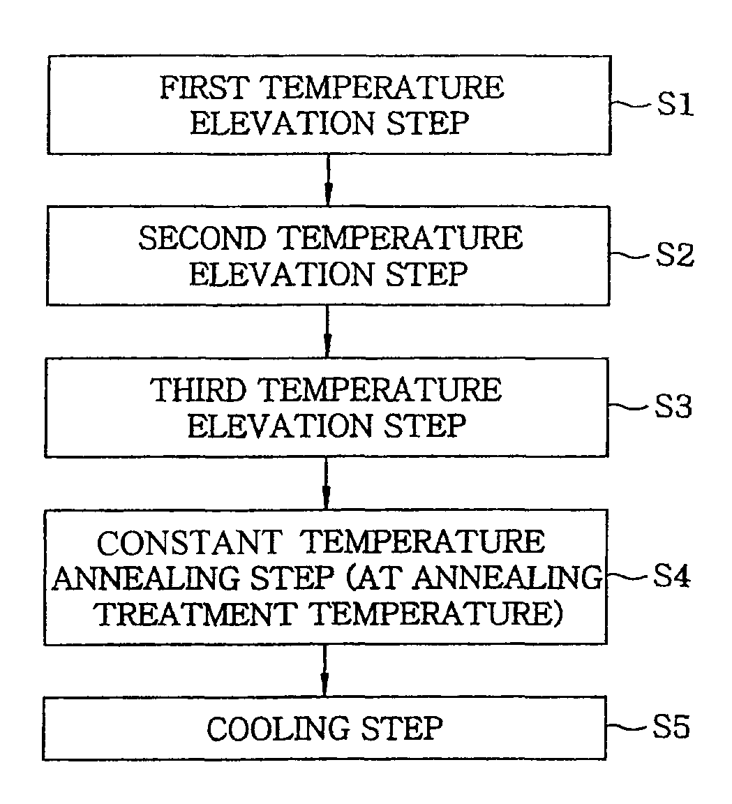
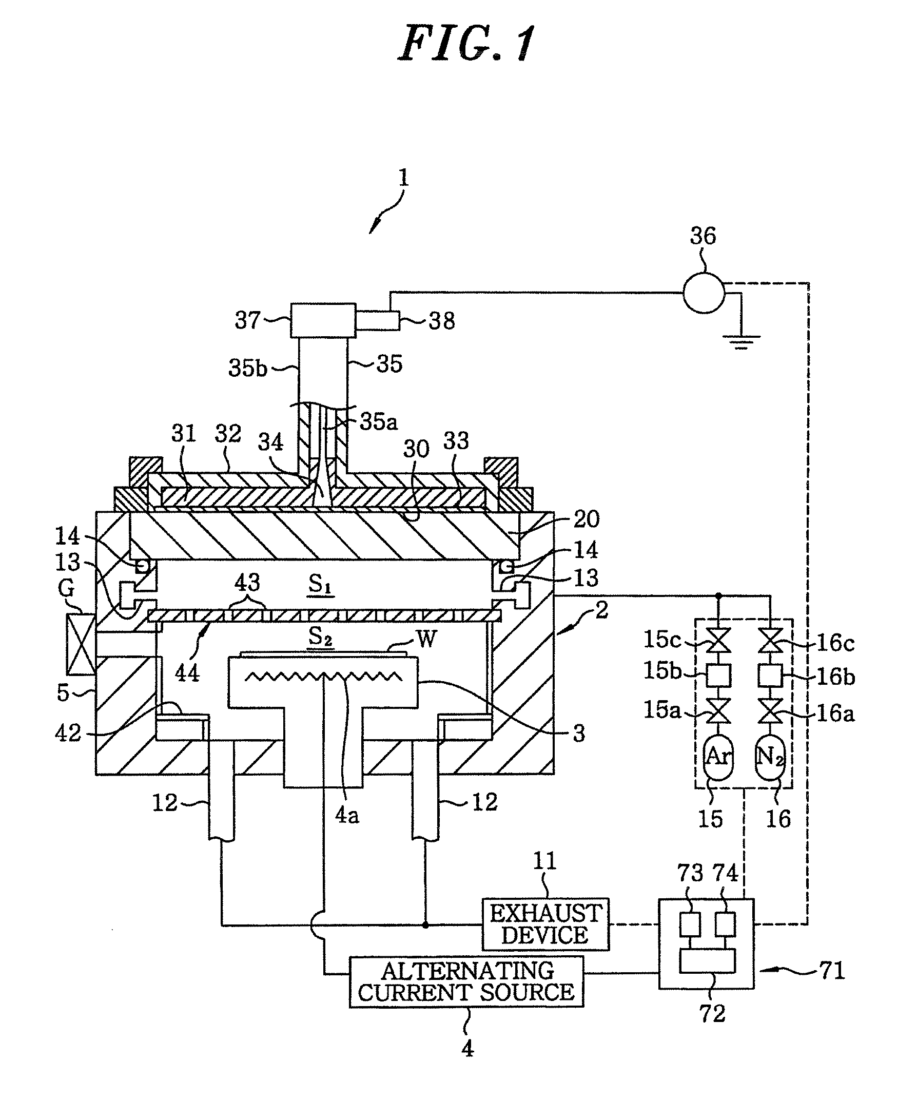
[0052]Hereinafter, embodiments of the present invention will be described. FIG. 1 shows a vertical section of a plasma processing apparatus 1 for performing a gate insulating film forming method in accordance with the present embodiment. The plasma processing apparatus 1 includes a upper portion-opened and bottom-closed cylindrical processing vessel 2 made of, e.g., aluminum, the processing vessel 2 being kept grounded. On a bottom portion of the processing vessel 2, there is provided a susceptor 3 that serves as a table for holding a substrate, e.g., a wafer W. The susceptor 3 is made of, e.g., aluminum, and is provided with a heater 4a therein. The heater 4a may be composed of, e.g., a resistor, and is adapted to generate heat as electric power is supplied from an alternating current source 4 provided outside the processing vessel 2. The heater 4a is capable of heating the wafer on the susceptor 3 to a predetermined temperature.

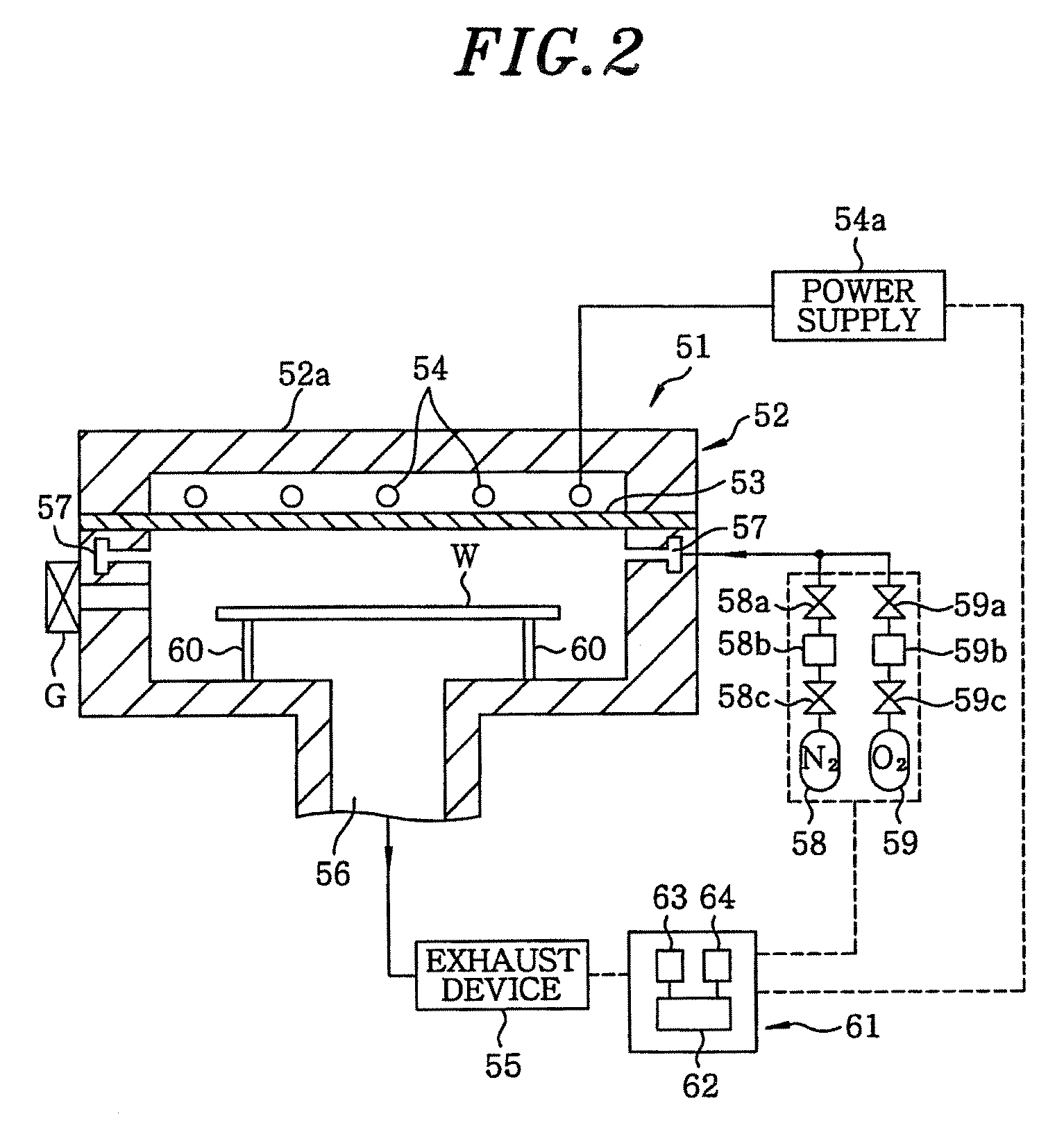
[0053]On the bottom portion of the processing vessel ...


PUM

PropertyMeasurementUnit
fixed temperatureaaaaaaaaaa
temperatureaaaaaaaaaa

Abstract

In a method for forming an insulating film by performing plasma nitriding process to an oxide film on a substrate and then by annealing the substrate in a process chamber (51), the substrate is annealed under a low pressure of 667 Pa or lower. The annealing is performed for 5 or 45 seconds. The plasma nitriding process is performed by microwave plasma by using a planar antenna whereupon a multitude of slot holes are formed.

Description

FIELD OF THE INVENTION[0001]The present invention relates to an insulating film forming method and a substrate processing method for performing an annealing treatment or other treatments to an object substrate such as a semiconductor wafer or the like.BACKGROUND OF THE INVENTION[0002]In a gate insulating film of recently semiconductor devices, e.g., a metal-oxide-semiconductor field-effect transistor (MOSFET), an oxynitride film is employed to prevent a so-called pass-through phenomenon. It is often the case that formation of the oxynitride film is performed by subjecting an oxide film to a plasma nitriding treatment.[0003]Meanwhile, it is a recent trend that the MOSFET itself becomes extremely miniaturized and, in concert with such miniaturization, the gate insulating film is controlled to be in an ultra-thin film region (of about 1.0 nm). In such a thin insulating film, however, there is a fear of degradation of a transistor-on current and reduction of an operating speed.[0004]In ...

Claims


Application Information

Patent Timeline
Patent Type & Authority Patents(United States)
IPC IPC(8): H01L21/469H01L21/31
CPCH01L21/3144H01L21/67115H01L21/67167H01L21/67207H01L21/0214H01L21/02252H01L21/02255H01L21/02332H01L21/0234
Inventor SATO, YOSHIHIRONAKAYAMA, TOMOEKOBAYASHI, HIROSHIOSAKI, YOSHINORITAKAHASHI, TETSURO
Owner TOKYO ELECTRON LTD
Why Eureka
Try Eureka