Ceramic substrate material, method for the production and use thereof, and antenna or antenna array

a substrate material and ceramic technology, applied in the direction of printed circuit dielectrics, porous dielectrics, decorative arts, etc., can solve the problems of low energy coupled into the material, wasteful consumption, and material described in de 100 43 194 a1 is not suitable for high frequency applications, and achieves a simple and cost-effective method and controllable

Inactive Publication Date: 2011-05-03
MICRO SYST ENG
View PDF34 Cites 7 Cited by
  • Summary
  • Abstract
  • Description
  • Claims
  • Application Information

AI Technical Summary

Benefits of technology

[0017]It is therefore the object of the present invention to specify a simple and cost-effective, and also reliable method for producing a ceramic substrate material for thick-film applications in the range of layer thicknesses above multiple tens of micrometers, preferably at layer thicknesses from approximately 20 to approximately 30 μm, which generates a substrate material having a low dielectric constant. Furthermore, the object comprises providing a corresponding thick ceramic substrate material which allows the use of LTCC technology. In addition, the object comprises specifying a suitable use of a ceramic substrate material of this type. Moreover, the object comprises specifying an antenna or on antenna array having a thick substrate material which is producible simply and cost-effectively.
[0019]The specified method is a very simple and cost-effective and also well controllable method for generating a ceramic substrate material having a low dielectric constant. It also does not cause the disadvantages specified above upon the use of hollow microbeads and leaves the LTCC method unchanged. In addition, due to the selective etching of the mantle areas, layers having a greater thickness in the range of multiple tens of micrometers, preferably layer thicknesses between approximately 20 μm and approximately 30 μm may be etched, because the mantle areas of the crystals and / or crystal agglomerates bond the adjacent crystals and crystal agglomerates to one another, and the etching agent thus penetrates along the mantle areas into the layer during the etching.

Problems solved by technology

With a low dielectric constant or permittivity, the largest possible part of the HF signal, of an antenna, for example, is emitted and little energy is coupled into the material and thus consumed wastefully.
The material described in DE 100 43 194 A1 is not suitable for applications at high frequencies, however.
However, the production of these materials is very complex.
Furthermore, a non-planar surface characteristic is to be expected, which particularly precludes the use in this field of thin-film technology having structural dimensions in the micrometer scale.
The production and the handling of a material composition of this type is also complex.
Above a proportion of 45 to 50 volume-% of the glass microbeads in the layer, however, the structural strength and the thermal resistance of the resulting insulating layers are negatively influenced.
They may fracture during the production method, so that the desired reduction of the dielectric constant is not achieved.
However, this is quite a complex production method.
In addition, the publication U.S. Pat. No. 4,867,935 discloses, as a further disadvantage of a layer having microbeads, that at too high a proportion (above 40%) of the microbeads, the air tightness of the resulting ceramic product worsens.
In addition, the surface roughness of the layer may become problematic during the further processing of the layer.
In contrast, at too low a proportion of the microbeads, the desired reduction of the dielectric constant may not be achieved.
The method described has the disadvantage that the LTCC method must be altered and additional layers must be used, which have a different shrinkage behavior than the remaining layers under certain circumstances.
The disadvantage of this method is that it is only suitable for very thin layers having a thickness of less than 1 μm.
Thin layers of this type are used in semiconductor circuits, but they are not suitable for use for antennas.
The etching of a thicker layer is not possible due to the lack of bonding of the particles to one another.

Method used


Image

  • Ceramic substrate material, method for the production and use thereof, and antenna or antenna array
  • Ceramic substrate material, method for the production and use thereof, and antenna or antenna array
  • Ceramic substrate material, method for the production and use thereof, and antenna or antenna array

Examples


examples

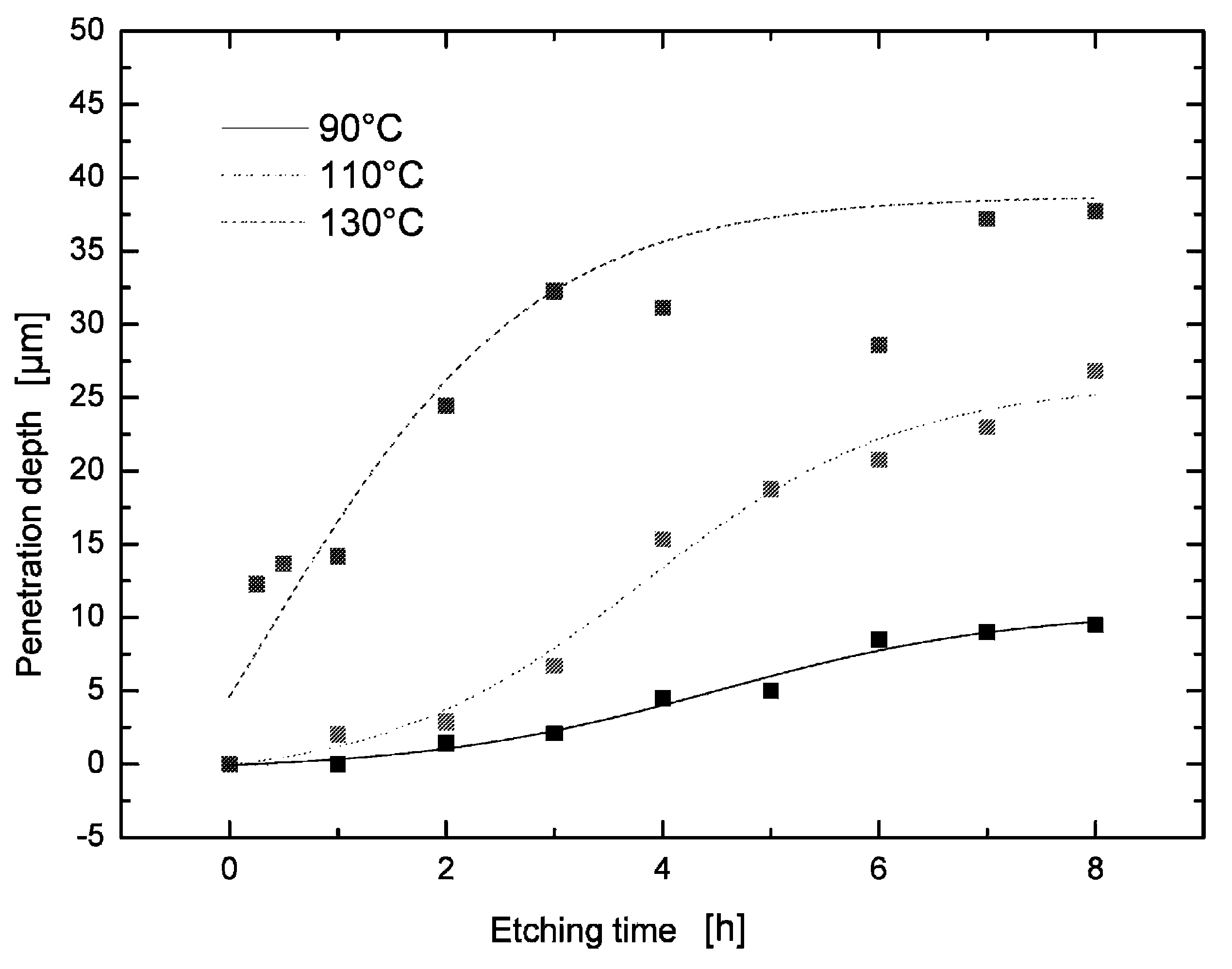
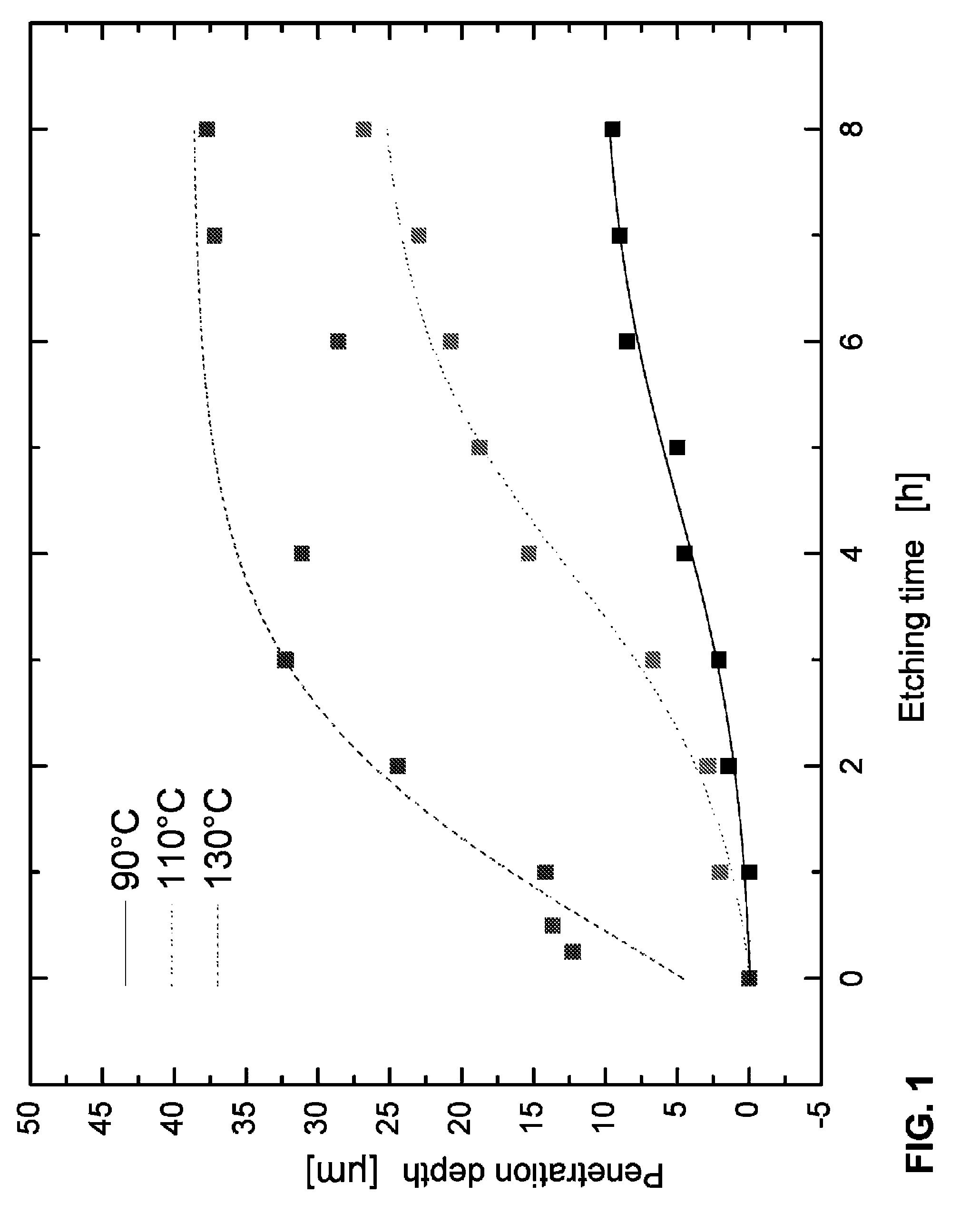
[0039]A substrate material having a first layer made of sintered glass ceramic, e.g., an LTCC tape having the composition 30% SiO2, 40% Al2O3, 4% CaO, 9% PbO, 2% B2O3+remainder—known under the product identification DP951, the composition 30% SiO2, 20% Al2O3, 3% CaO, 5% SrO, 17% BaO, 5% ZnO+remainder—known as “Heraeus Tape”—or the composition approximately 50% Al2O3, approximately 15% B2O3, approximately 15% La2O3, +remainder, which is known under the product identification DP943 of Hereaus, is laid in a suitable etching solution (e.g., phosphoric acid for DP951, “Heraeus Tape”, and DP943) at a temperature of 110° C. for the porosification. The porosification procedure may alternatively also be performed using KOH (potassium hydroxide solution) of a concentration of approximately 40% at a temperature in the range of 80° C.

[0040]The curve illustrated in the diagram of FIG. 1 shows the dependence of the penetration depth of the etching solution phosphoric acid into the volume of the g...


PUM

PropertyMeasurementUnit
thicknessaaaaaaaaaa
temperaturesaaaaaaaaaa
temperatureaaaaaaaaaa

Abstract

A method for producing a ceramic substrate material having a first layer and possibly a further layer is specified. The first layer comprises at least one first component made of a crystalline ceramic material and / or a glass material as a matrix and a second component made of a further crystalline ceramic material, which is provided in the matrix. An etching step is performed, mantle areas of the crystals and / or crystal agglomerates of the second component being etched selectively in the first layer to generate a cavity structure in the first layer. The present invention also relates to a corresponding ceramic substrate material, an antenna or an antenna array, and the use of the ceramic substrate material for an antenna or an antenna array.

Description

[0001]This application takes priority from German Patent Application DE 10 2007 020 888.1, filed 4 May 2007, the specification of which is hereby incorporated herein by reference.BACKGROUND OF THE INVENTION[0002]1. Field of the Invention[0003]The invention relates to a method for producing a ceramic substrate material having a first layer and possibly a further layer, the first layer comprising at least one first component made of a crystalline ceramic material and / or a glass material as a matrix and a second component made of a crystalline ceramic material which is present in the matrix. Furthermore, the invention relates to a ceramic substrate material having a first layer and possibly a further layer, the first layer comprising a least one first component made of a crystalline ceramic material and / or a glass material as a matrix. In addition, the present invention relates to the use of a ceramic substrate material of this type and an antenna or an antenna array.[0004]2. Descripti...

Claims


Application Information

Patent Timeline
Patent Type & Authority Patents(United States)
IPC IPC(8): B32B5/18C23F1/00
CPCH05K1/024C04B41/009C04B41/91H01Q1/38C04B41/5353C03C15/00C04B35/10C04B35/00Y10T428/24479H05K1/0306Y10T428/24562C04B2111/00844H05K2201/0116H05K3/002Y10T428/249969Y10T428/24997
Inventor SCHWANKE, DIETERBITTNER, ACHIMSCHMID, ULRICHHARNACK, MIRCO
Owner MICRO SYST ENG
Why Eureka
Try Eureka