
Phase shift mask blank, phase shift mask, and method for manufacturing phase shift mask blank

a technology of phase shift mask and mask blank, which is applied in the field of phase shift mask, and the method of manufacturing phase shift mask blank, can solve the problems of difficult to repair the defects of the engraved portion of the substrate, the difficulty of controlling the accuracy of the transparent substrate, and the difficulty of meeting the requirements of pattern collapse and pattern accuracy, so as to achieve the effect of satisfying the pattern accuracy requirement and improving the controllability of phase differen

Active Publication Date: 2011-05-03
HOYA CORP
View PDF3 Cites 7 Cited by
  • Summary
  • Abstract
  • Description
  • Claims
  • Application Information

AI Technical Summary

Benefits of technology

According to the preferred aspects of the present invention, even in the OPC pattern that is indispensable for the semiconductor devices of 32 nm node generation and beyond, the pattern can be prevented from collapsing and the pattern accuracy requirement can be satisfied.
According to the preferred aspects of the present invention, the transmittance at a wavelength (257 nm) of a defect inspection apparatus is equal to or less than 60%, the reflectance at a wavelength (678 nm) of light that is used for etching end point detection when the phase shift film is patterned by etching is equal to or greater than 20%, and controllability of phase difference is improved. As a result, it is possible to provide a phase shift mask and a phase shift mask blank that can be inspected for defects and can be used in semiconductor devices of the 32 nm node generation and beyond.

Problems solved by technology

The problems associated with the engraved phase shift mask, which is the former of the above-described two masks, are that the transparent substrate is difficult to control accurately so as to obtain a phase difference of 180° and that defects of the engraved portions of the substrate are difficult to repair.
The resultant problem is that the requirements relating to pattern collapse and pattern accuracy are difficult to meet in the semiconductor devices of a 32 nm node generation and beyond for which an OPC pattern with a minimum pattern width of equal to or less than 50 nm is indispensable.

Method used


Image

  • Phase shift mask blank, phase shift mask, and method for manufacturing phase shift mask blank
  • Phase shift mask blank, phase shift mask, and method for manufacturing phase shift mask blank
  • Phase shift mask blank, phase shift mask, and method for manufacturing phase shift mask blank

Examples


example 1

A phase shift mask blank of Example 1 was a halftone phase shift mask blank in which a phase shift film composed of MoSiNO and a light-shielding film were provided on a 6025 (size: 6 inch×6 inch, thickness 0.25 inch) transparent substrate composed of synthetic quartz, wherein the light-shielding film was composed of a Cr-containing material and had formed on the surface thereof a surface antireflection layer having an antireflection function that enables the suppression of reflection of light returning from the transferred substrate side, with respect to the wavelength of ArF excimer laser beam.

The phase shift film and light-shielding film in the phase shift mask blank of Example 1 were formed with a DC magnetron sputtering apparatus.

The phase shift film composed of MoSiNO was formed on the transparent substrate by reactive sputtering by using a mixed target including Mo and Si (a Mo content to a total content of Mo and Si was 4%; relative density was equal to or greater than 98%) a...

example 2

A halftone phase shift mask blank and a halftone phase shift mask with a transmittance with respect to the ArF excimer laser beam of 14.8% were fabricated in the same manner as in Example 1, except that a mixed gas atmosphere of Ar gas, N2 gas, O2 gas, and He gas (Ar: 11 sccm, N2: 50 sccm, O2: 4.2 sccm, and He: 100 sccm) was used as a sputtering gas for forming the phase shift film in the process of the above-described Example 1.

The phase shift film had a transmittance in an ArF excimer laser (wavelength 193 nm) of 14.8% and a phase difference of 176.8° (measurements were conducted with a phase shift amount measurement device MPM193 manufactured by Lasertec Corporation).

The refractive index (n) of the phase shift film was 2.44, the extinction coefficient (k) was 0.38, and the film thickness was 68 nm.

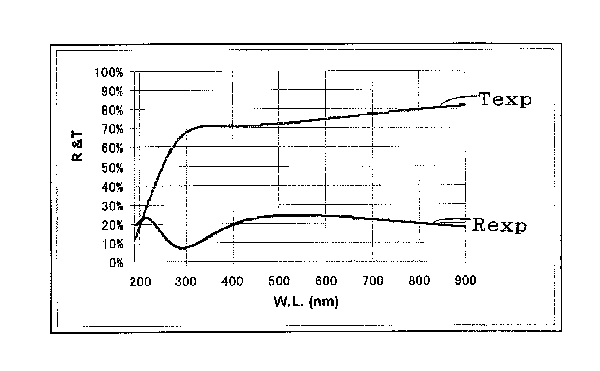
The transmittance and reflectance characteristics of the phase shift film are shown in FIG. 4. The transmittance at 257 nm, which is an inspection light wavelength of mask defect inspec...

example 3

A halftone phase shift mask blank and a halftone phase shift mask with a transmittance with respect to the ArF excimer laser beam of 13.4% were fabricated in the same manner as in Example 2, except that the sputtering gas used for forming the phase shift film in the above-described Example 1 was changed to a mixed gas atmosphere of Ar gas, N2 gas, and He gas (Ar: 10.5 sccm, N2: 55 sccm, and He: 100 sccm) and a film for an etching mask composed of MoSiN and having a thickness of 15 nm was formed on the light-shielding film.

The phase shift film had a transmittance in an ArF excimer laser (wavelength 193 nm) of 13.4% and a phase difference of 160.0° (measurements were conducted with a phase shift amount measurement device MPM193 manufactured by Lasertec Corporation).

The refractive index (n) of the phase shift film was 2.53, the extinction coefficient (k) was 0.45, and the film thickness was 58.0 nm.

The composition analysis of the phase shift film was conducted by Auger electron spectro...


PUM


Abstract

Problem: There is a demand for a phase shift mask that makes it possible to decrease the film thickness of the phase shift film, can satisfy the requirement relating to pattern accuracy, without collapsing the OPC pattern, and enables control of optical characteristics and pattern defect inspection, and also for a phase shift mask blank as an original plate for such a phase shift mask.Means for Solving the Problems: A phase shift mask blank of the present invention has, on a transparent substrate, a phase shift film including, as main components, a metal, silicon (Si) and nitrogen (N), having optical characteristics of a transmittance of equal to or greater than 9% and equal to or less than 30% with respect to a wavelength of the ArF excimer laser beam and a phase difference of equal to or greater than 150° and less than 180°, and a light-shielding film formed on the phase shift film. A thickness of the phase shift film is equal to or less than 80 nm, and a refractive index (n) with respect to the wavelength of the ArF excimer laser beam is equal to or greater than 2.3, and an extinction coefficient (k) is equal to or greater than 0.28.

Description

FIELD OF THE INVENTIONThe present invention relates to a phase shift mask blank, a phase shift mask, and a method for manufacturing a phase shift mask blank.DESCRIPTION OF THE RELATED ARTThe advantages of increasing the degree of integration of semiconductor devices and the like include improvement of performance and functions (high-speed operation or reduced power consumption etc.) and cost reduction, and miniaturization of circuit patterns of semiconductor devices has been accelerated. Lithography is a technique that aids in miniaturizing the circuit patterns of semiconductor devices, and transfer masks that are used for transferring circuit patterns have occupied, together with exposure devices and resist materials, a highly important place.Development of semiconductor devices of a semiconductor device design rule of 32 nm node and 22 nm node has been advances in recent years. A minimum line width formed in such semiconductor devices corresponds to 1 / 9 to ⅙ the wavelength (λ: 193...

Claims


Application Information

Patent Timeline
IPC IPC(8): G03F1/00
CPCG03F1/54G03F1/32G03F1/26
Inventor NOZAWA, OSAMUHASHIMOTO, MASAHIRO
Owner HOYA CORP
Features
  • Generate Ideas
  • Intellectual Property
  • Life Sciences
  • Materials
  • Tech Scout
  • Unparalleled Data Quality
  • Higher Quality Content
  • 60% Fewer Hallucinations
Learn More