Low voltage interface circuit

a low-voltage interface and circuit technology, applied in the direction of logic circuit coupling/interface arrangement, pulse technique, instruments, etc., can solve the problems of gate oxide degradation or breakdown, circuit failure, etc., and achieve low-voltage interface high-efficiency, low-voltage

Active Publication Date: 2011-06-07
CYPRESS SEMICON CORP
View PDF95 Cites 17 Cited by
  • Summary
  • Abstract
  • Description
  • Claims
  • Application Information

AI Technical Summary

Benefits of technology

[0012]One unique aspect of the invention is the use of a current sense amplifier (ISA) within a low voltage interface circuit. For example, the current sense amplifier may be included within the interface circuit for clamping the voltage levels present at the drain terminals of the input transistors to a particular voltage level. By clamping the drain voltages to a relatively high level (e.g., about 1.0V or above), the current sense amplifier may (i) avoid gate oxide degradation / breakdown of the low voltage transistors contained within the interface circuit, and (ii) eliminate the need for inserting a level clipping circuit (including, e.g., high voltage transistors and high voltage power supplies) within the signal path between an input node of the interface circuit and the low voltage input transistors. The current sense amplifier, therefore, enables a highly robust, low voltage interface circuit to be provided herein for converting a relatively high input voltage into a relatively low output voltage using only low voltage transistors and a single, low voltage power supply.
[0013]In general, low voltage transistors may be formed with thinner gate oxides and / or different source / drain dopants and / or concentrations than high voltage transistors. Low voltage transistors may also be somewhat smaller than their high voltage counterparts. As such, low voltage transistors may be optimized for operating within a relatively lower voltage range than high voltage transistors of the same process technology. In some embodiments, a low voltage transistor may be described as one, which is configured for operating within a relatively low voltage range of about 0.0V to about 1.8V (for older CMOS process technologies), or about 0.0V to about 1.45V (for new CMOS process technologies). However, the designation of high and low operating voltages is process dependent and, therefore, may vary in other embodiments of the invention. Regardless, including only low voltage transistors within the interface circuit enables the circuit to be adequately supplied with a single, low voltage power supply (e.g., about 1.45V and below) and avoids the design difficulties typically involved in multiple power supply systems.

Problems solved by technology

However, a problem often arises when a high voltage input signal (e.g., above about 1.45 V for CMOS process technologies) is supplied to a low voltage transistor.
In other words, gate voltages in excess of about 1.45V tend to overstress the thinner gate oxides of low voltage CMOS transistors, often resulting in gate oxide degradation or breakdown.
Performance issues arise when the gate oxide begins to degrade, with circuit failure occurring when the gate oxide reaches breakdown.

Method used


Image

  • Low voltage interface circuit
  • Low voltage interface circuit
  • Low voltage interface circuit

Examples


Embodiment Construction

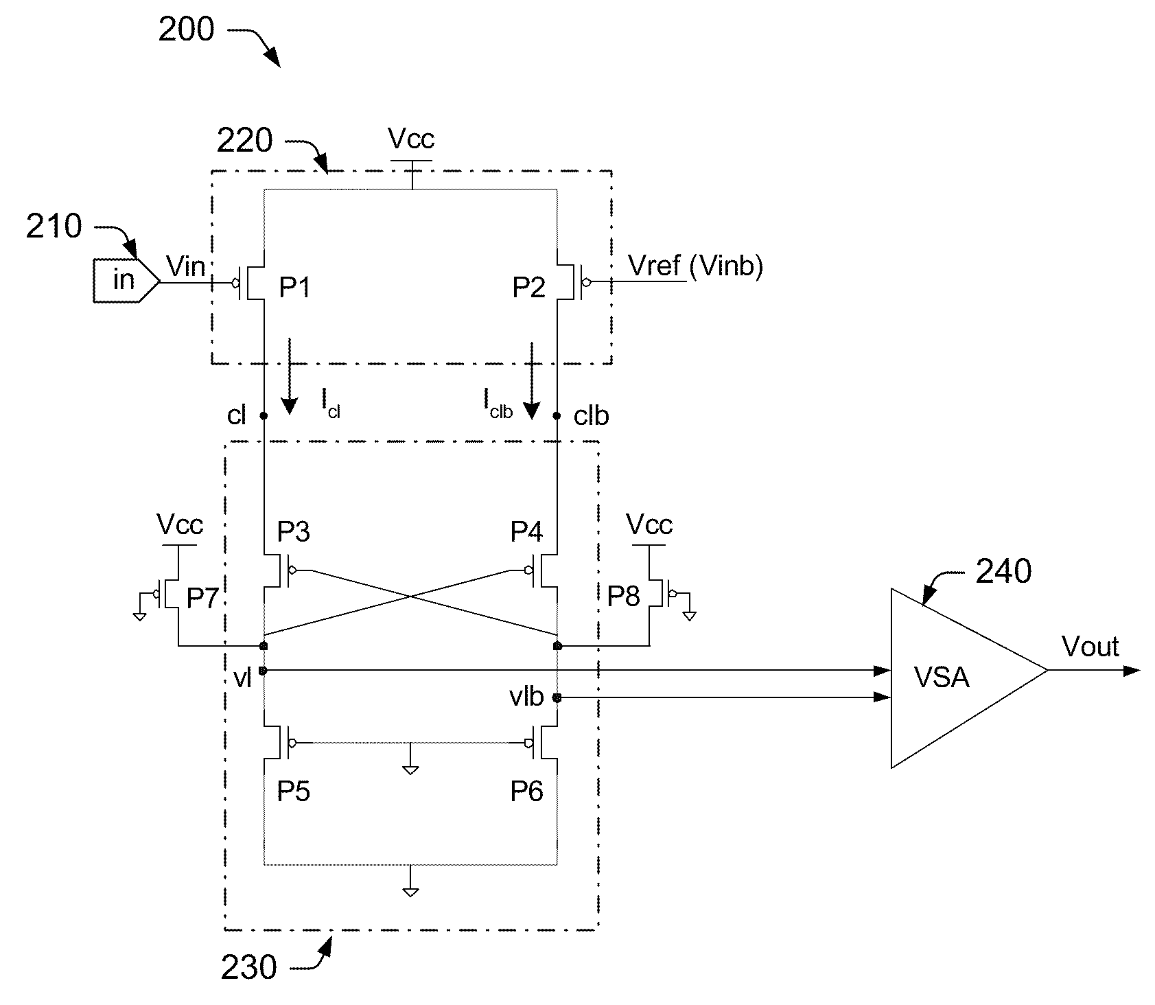
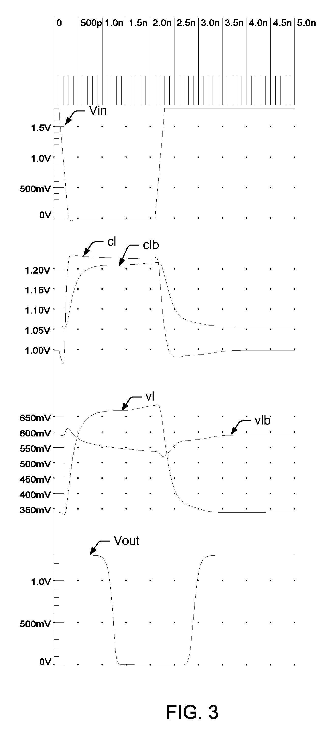
[0022]Turning now to the drawings, FIG. 1 illustrates one embodiment of an interface circuit 100 in which a level clipping circuit 120 is arranged within the signal path between an input node 110 and buffer portion 130 of the interface circuit. To accommodate relatively low internal power supply levels (e.g., below about 1.45V), buffer portion 130 may typically include a pair of low voltage transistors (not shown in FIG. 1). In some cases, the low voltage transistors may be arranged as a differential pair for receiving an input signal and a reference signal (in the case of a single-ended interface circuit) or a pair of complementary input signals (in the case of a differential interface circuit).

[0023]As used herein, transistors designated as low voltage may be somewhat smaller than so-called high voltage transistors, and may be formed with substantially thinner gate oxides and / or different source / drain dopants (and / or concentrations). As such, low voltage transistors may operate wi...


PUM


Abstract

An improved interface circuit is provided herein for translating a relatively high input voltage into a relatively low output voltage using only low voltage transistors and a single, low voltage power supply. According to one embodiment, the interface circuit includes a power supply, a pair of input transistors with source terminals coupled together for receiving a relatively low voltage from the power supply, and a current sense amplifier with a pair of input terminals, each coupled to a drain terminal of a different one of the pair of input transistors for receiving a pair of differential currents and for generating a pair of differential voltages therefrom.

Description

PRIORITY CLAIM[0001]This application claims priority to U.S. Provisional Application No. 60 / 675,762 entitled “Low Voltage Interface Circuit,” filed Apr. 28, 2005.BACKGROUND OF THE INVENTION[0002]1. Field of the Invention[0003]This invention relates to interface circuit design and, more particularly, to an input buffer design including low voltage transistors and a single low voltage power supply.[0004]2. Description of the Related Art[0005]The following descriptions and examples are not admitted to be prior art by virtue of their inclusion within this section.[0006]A current trend in integrated circuit (IC) design is that internal power supply levels continue to fall, while external power supply levels remain substantially unchanged. For example, extended high speed transistor logic (eHSTL) with voltage swings between about 0.0V and 1.8V is often used for inter-IC signaling, even though the IC's themselves may operate at significantly lower levels (e.g., about 1.2V to about 1.8V). T...

Claims


Application Information

Patent Timeline
Patent Type & Authority Patents(United States)
IPC IPC(8): H03K19/094
CPCH03K3/356182
Inventor PENG, TAOZHANG, XIAOHU
Owner CYPRESS SEMICON CORP
Why Eureka
Try Eureka