Compound semiconductor light-emitting device and method for manufacturing the same

a light-emitting device and semiconductor technology, applied in semiconductor devices, semiconductor/solid-state device details, electrical apparatus, etc., can solve the problems of easy generation of burrs, difficult control, and light emitted in the light-emitting layer is not extracted to the outside, and achieve excellent etching properties, good yield, and excellent transparency

Active Publication Date: 2011-07-05
TOYODA GOSEI CO LTD
View PDF13 Cites 4 Cited by
  • Summary
  • Abstract
  • Description
  • Claims
  • Application Information

AI Technical Summary

Benefits of technology

[0010]In light of the above problems, the present invention has been made and an object thereof is to provide a compound semiconductor light-emitting device that is excellent in manufacturing yield, and has high light emission output, and a method for manufacturing the same.
[0038]According to the present invention, it is possible to manufacture a compound semiconductor light-emitting device, that shows good yields in the manufacturing process, by using an amorphous IZO film having excellent etching properties. It is also possible to convert an amorphous state into a structure containing a crystal by subjecting the IZO film to a heat treatment (hereinafter referred to as “crystallization”). The crystallized IZO film is excellent in transparency as compared with the amorphous ITO film, and thus a compound semiconductor light-emitting device having high light emission output by crystallizing the IZO film after an etching treatment can be obtained.

Problems solved by technology

Therefore, electric current is injected only into a semiconductor directly under an electrode, and light emitted in the light-emitting layer is not extracted to the outside since the light is blocked by the electrode.
In wet etching using such a strong acid, etching takes place at a high rate, and thus it is difficult to control and burrs are easily generated at the edge portion of the ITO.
Further, overetching easily occurs, resulting in poor yield.
Therefore, burrs caused by etching and overetching do not easily occur.
However, the amorphous IZO film is inferior in transparency compared with the heat-treated ITO film, and therefore shows low output of the light-emitting device.
Furthermore, there is a problem that the device has high drive voltage, since contact resistance with a p-type GaN layer is high, and the device is inferior in water resistance and chemical resistance, since it is amorphous, which results in a decrease in manufacturing yield after forming the ITO film and reliability of the device.

Method used


Image

  • Compound semiconductor light-emitting device and method for manufacturing the same
  • Compound semiconductor light-emitting device and method for manufacturing the same
  • Compound semiconductor light-emitting device and method for manufacturing the same

Examples


example 1

Manufacture of Gallium Nitride-Based Compound Semiconductor Light-emitting Device

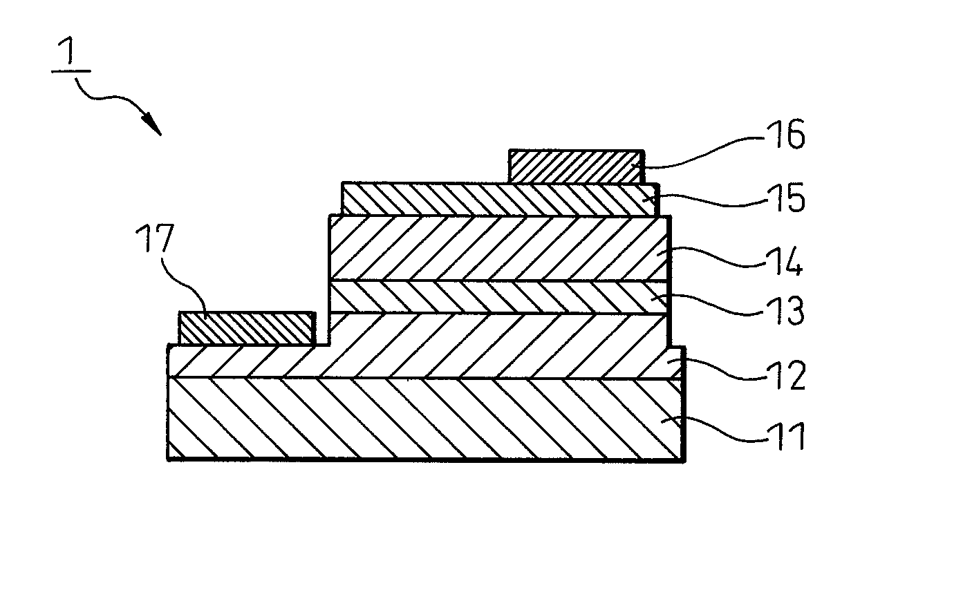
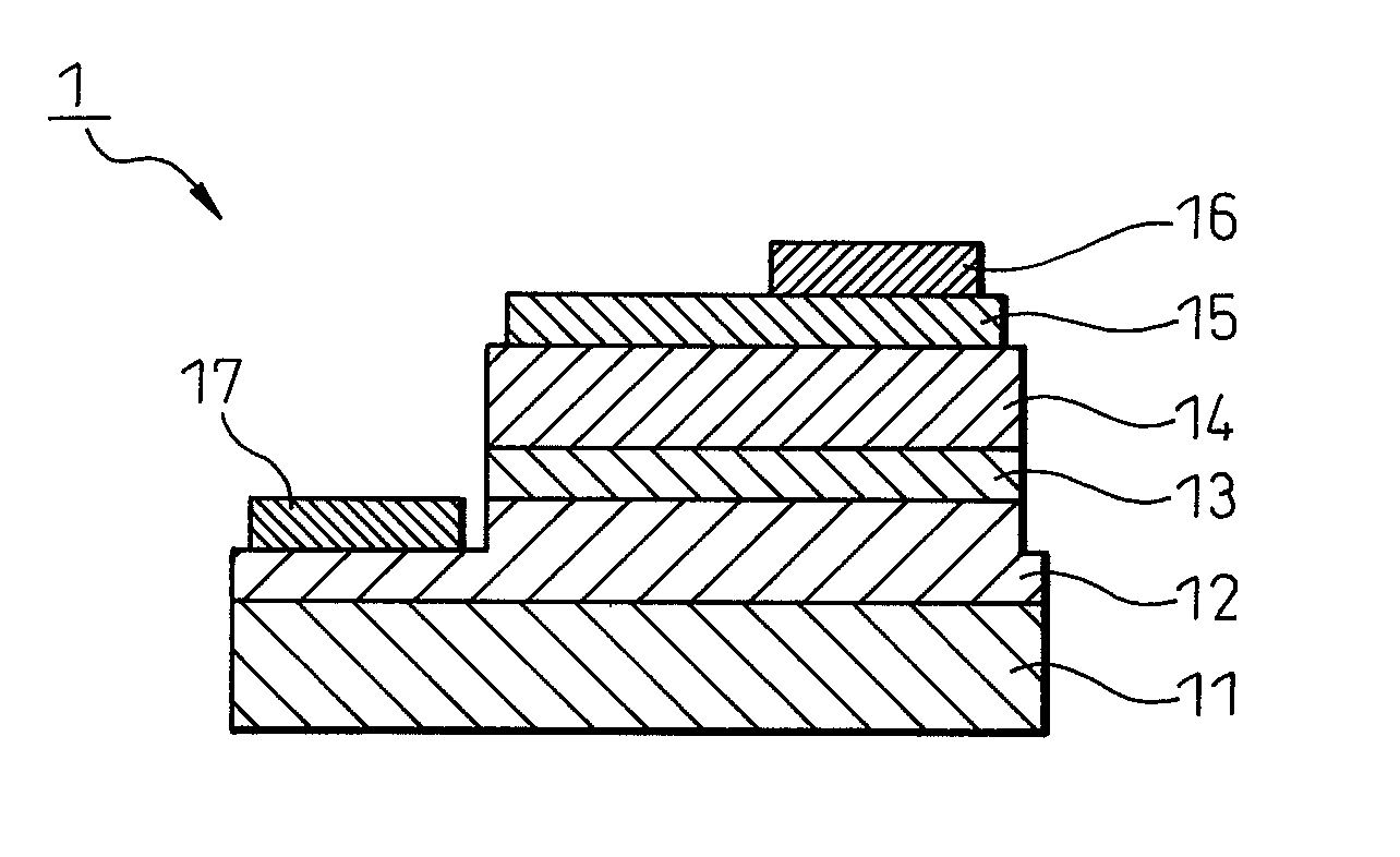
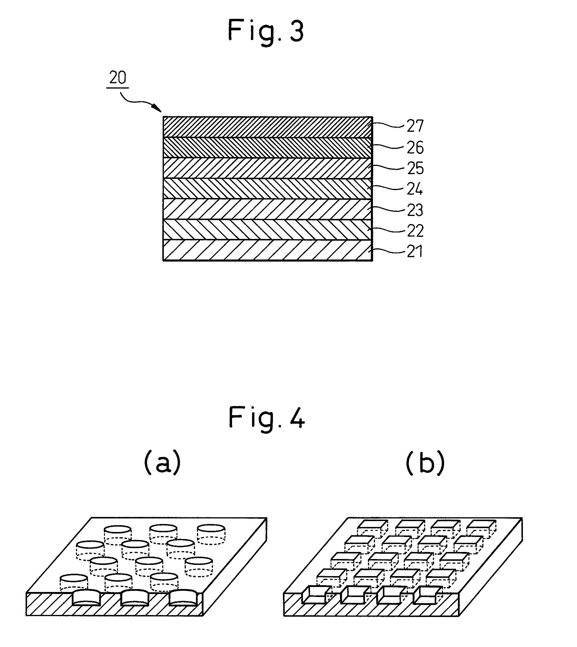
[0105]In FIG. 3, a schematic sectional view of a semiconductor wafer comprising a gallium nitride-based compound semiconductor layer manufactured so as to be used in gallium nitride-based compound semiconductor light-emitting device of this example is shown. In FIG. 1 and FIG. 2, a schematic sectional view and a plan view of the gallium nitride-based compound semiconductor light-emitting device manufactured in this example are shown. Description will now be made with reference to these drawings.

[0106]A stacked structure of a gallium nitride-based compound semiconductor wafer 20 was formed by sequentially forming, on a substrate 21 made of the c-surface (crystal (0001) face) of sapphire, an undoped GaN underlying layer (2 μm in thickness) 22, a Si-doped n-type GaN contact layer (2 μm in thickness, carrier concentration: 1×1019 cm−3) 23, a Si-doped n-type Al0.07Ga0.93N clad layer (12.5 nm in thickness, ca...

example 5

[0119]In the same manner as in Example 1, except that the surface that is not contacted with the p-type semiconductor layer of the IZO film is subjected to uneven working, a gallium nitride-based compound semiconductor light-emitting device was manufactured, and then evaluated in the same manner as in Example 1.

[0120]The uneven working step was performed before the heat treatment of the IZO film and wet etching was performed using the ITO-07 etching solution in the same manner as in the case of patterning of the IZO film. The uneven shape is a cylindrical recess shape measuring 2 μm in diameter and 150 nm in depth. Cylindrical recesses were arranged zigzag at a center pitch of 3 μm. Vf of the resulting gallium nitride-based compound semiconductor light-emitting device was 3.23 V, and Po was 13.5 mW.

examples 6 and 7

[0121]In the same manner as in Example 5, except that the depths of the cylindrical recesses were respectively adjusted to 200 nm and 250 nm, gallium nitride-based compound semiconductor light-emitting devices were manufactured, and then evaluated in the same manner as in Example 1.

[0122]In FIG. 10, a relation between the depth of the recesses on the surface of the IZO film, and Vf and Po of the gallium nitride-based compound semiconductor light-emitting device is shown. The abscissa denotes the depth (nm) of the recesses on the surface of the IZO film while the ordinate denotes Vf (V) of the gallium nitride-based compound semiconductor light-emitting device and Po (mW) of the gallium nitride-based compound semiconductor light-emitting device. When the depth of the recesses on the surface of the IZO film is 0, it shows that uneven working is not performed (Example 1).

[0123]As is apparent from the results shown in FIG. 10, as the depth of the recesses formed on the surface that is no...


PUM


Abstract

A compound semiconductor light-emitting device which includes an n-type semiconductor layer, a light-emitting layer and a p-type semiconductor layer, that are made of a compound semiconductor, formed on a substrate, the n-type semiconductor layer and the p-type semiconductor layer are stacked so as to interpose the light-emitting layer therebetween, a first conductive transparent electrode and a second conductive electrode. The first conductive transparent electrode is made of an IZO film containing an In2O3 crystal having a bixbyite structure. Also discussed is a method of manufacturing the device.

Description

TECHNICAL FIELD[0001]The present invention relates to a compound semiconductor light-emitting device, particularly a gallium nitride-based compound semiconductor light-emitting device, and also relates to a compound semiconductor light-emitting device having high light emission output and a method for manufacturing the same.BACKGROUND ART[0002]A pn-junction type light-emitting diode (LED) is known as one example of a compound semiconductor light-emitting device. For example, a GaP-based LED is known, in which a GaP layer formed by epitaxial growth of a gallium phosphide (GaP) single crystal on a substrate is used as a light-emitting layer. A red range and orange to green range LED comprising an aluminum gallium arsenide mixed crystal (composition formula: AlXGaYAs (0≦X, Y≦1 and X+Y=1) or an aluminum gallium indium phosphide mixed crystal (composition formula: AlXGaYInZP (0≦X,Y,Z≦1, X+Y+Z=1) as a light-emitting layer is also known. A short wavelength (near ultraviolet, blue or green ...

Claims


Application Information

Patent Timeline
Patent Type & Authority Patents(United States)
IPC IPC(8): H01L33/00H01L33/32H01L33/22H01L33/38H01L33/42
CPCH01L33/42H01L2933/0016H01L33/38H01L33/32H01L2924/181H01L2224/48091H01L2224/48247H01L2224/48257H01L2224/45144H01L2224/49107H01L2924/00012H01L2924/00014
Inventor FUKUNAGA, NAOKISHINOHARA, HIRONAO
Owner TOYODA GOSEI CO LTD
Why Eureka
Try Eureka