eFuse containing SiGe stack

a technology of efuse and stack, applied in the field of efuse, can solve the problems of reliability concerns, damage to the device passivation layer, hole in the passivation layer, etc., and achieve the effects of improving efuse programming, reducing thermal conductivity, and reducing melting temperatur

Inactive Publication Date: 2011-08-23
GLOBALFOUNDRIES INC
View PDF20 Cites 10 Cited by
  • Summary
  • Abstract
  • Description
  • Claims
  • Application Information

AI Technical Summary

Benefits of technology

[0016]The fuse of the present invention has the advantage that it can be successfully programmed over a wide range of programming voltages and time. The thermal conductivity of Si is 1.3 W / cm K and that of SiGe is 0.1 W / cm K. The SiGe layer below silicide provides much improved thermal insulation required for successful programming without special control effort.
[0019]Thermal diffusivity of Si is 0.8 cm2 / sec and that of SiGe is 0.36 cm2 / sec. Electromigration, which is the diffusion of atoms due to electron wind force, is easier with the lower melting temperature of SiGe compared to Si. The SiGe layer below silicide improves eFuse programming in at least three ways: lower thermal conductivity, lower thermal diffusivity, and lower melting temperature. The maximum temperature in the fuse link (for the same geometry and current density) is achieved much easier with SiGe layer below silicide. The voltage, current and time needed to program the inventive fuse are small, which results in significant savings in area.

Problems solved by technology

This and other similar approaches can result in damage to the device passivation layer, and thus, lead to reliability concerns.
For example, the process of blowing the fuse can cause a hole in the passivation layer when the fuse material is displaced.
However, this type of fuse device can result in damage to surrounding structure and / or suffers from unreliable sensing because of the inconsistent nature of the rupture process and the relatively small change typically offered in the programmed resistance.
Further, these type of devices may not be viable for use with many of the latest process technologies because of the required programming potentials, i.e. current flow and voltage levels over a requisite amount of time.
This sometimes results in a programmed fuse being sensed incorrectly and, thus, leading to the failure of the chip.

Method used


Image

  • eFuse containing SiGe stack
  • eFuse containing SiGe stack
  • eFuse containing SiGe stack

Examples


embodiment one

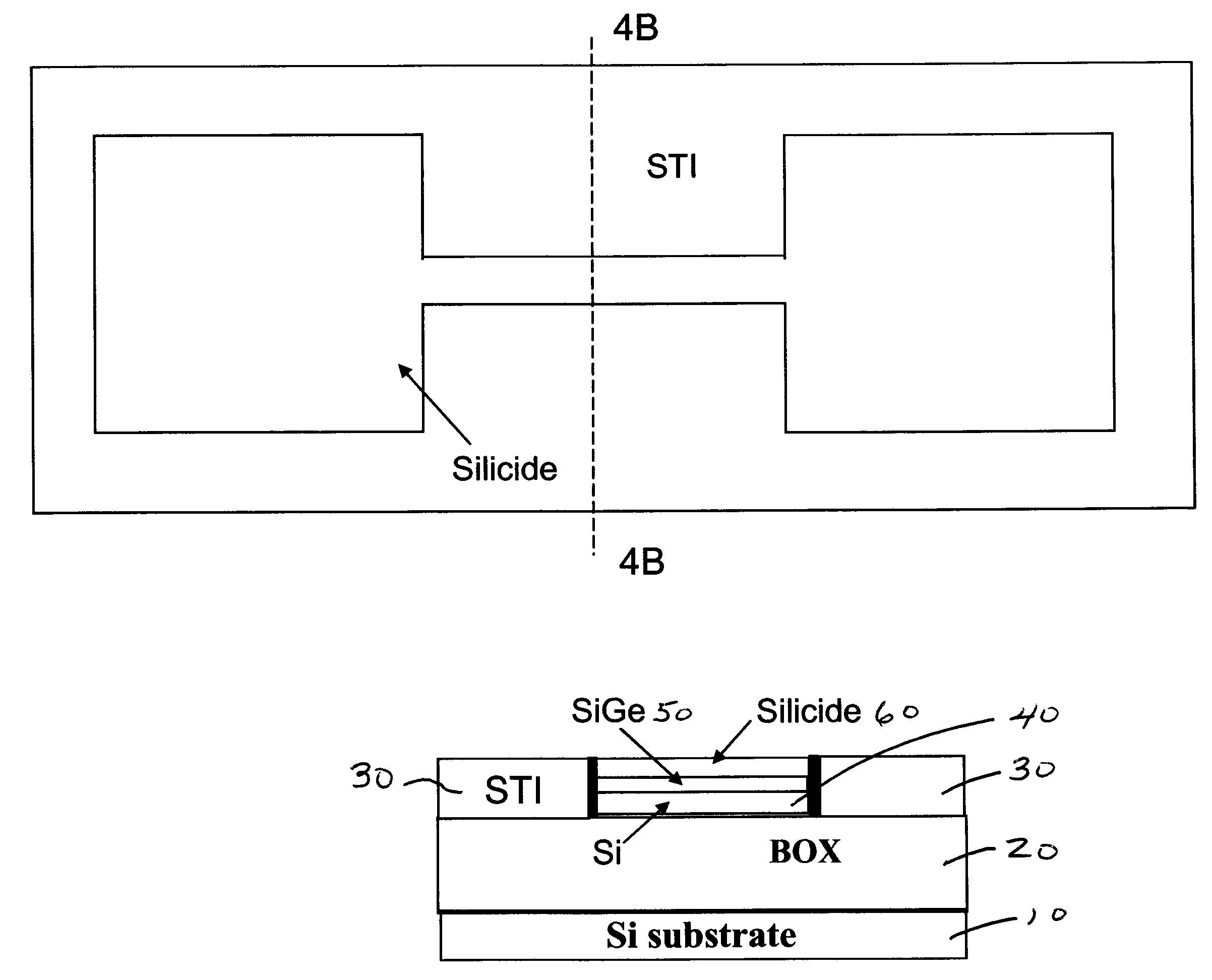
[0048]FIGS. 2A and 2B illustrate a plan view and a cross-sectional view of an intermediate structure for an electrically programmable fuse (hereinafter referred to as an eFuse) after a conventional shallow trench isolation (STI) formation, by well known techniques which need not be further described in accordance with the first embodiment of the present invention. A pad oxide (˜50 A) 100 is conventionally grown on an SOI wafer 10, 20, 40 and a pad nitride (between 1000 A-2000 A) 110 is deposited as shown using LPCVD (low pressure chemical vapor deposition). After an area (which will form STI regions) is patterned (conventionally) and etched using RIE (reactive ion etching), a thin oxide liner 120 (˜100 A) is thermally grown in a furnace (not shown) and a thin nitride liner (not shown in the figures) is deposited using LPCVD. After that, an oxide to form the STI region is deposited conventionally either by LPCVD or HDPCVD (high density plasma chemical vapor deposition). The extra oxi...

embodiment two

[0053]Now FIGS. 6, 11, 12 and 13 illustrate embodiment 11. Shallow trench isolation is formed following standard CMOS processing. A polycrystalline Si layer 401 and a polycrystalline SiGe layer 501 are deposited as poly conductor layers (by LPCVD). The structure is patterned while poly conductors are patterned by lithography and RIE. After that, nitride spacers 601 are formed by depositing nitride and etching using RIE. The top down and cross sections after the nitride spacer formation are shown in FIGS. 6A and 6B.

[0054]This eFuse structure with more thermally insulating SiGe below enables very easy achievement of a high and uniform final resistance, thus avoiding deleterious effects such as insufficient programming, rupture or agglomeration and avoiding collateral damage to adjacent devices. The inventive fuse structure (e.g. EMBODIMENT ONE or TWO) thus advantageously permits lower programming voltage / current and / or programming time. The eFuse structure can be formed using standard...


PUM

PropertyMeasurementUnit
thermal conductivityaaaaaaaaaa
Thermal diffusivityaaaaaaaaaa

Abstract

An eFuse, includes: a substrate and an insulating layer disposed on the substrate; a first layer including a single crystal or polycrystalline silicon disposed on the insulating layer; a second layer including a single crystal or polycrystalline silicon germanium disposed on the first layer, and a third layer including a silicide disposed on the second layer. The Ge has a final concentration in a range of approximately five percent to approximately twenty-five percent.

Description

BACKGROUND OF THE INVENTION[0001]1. Technical Field of the Invention[0002]The invention relates generally to the field of integrated circuits and, more particularly, to eFuse.[0003]2. Description of Related Art[0004]In integrated circuits including CMOS integrated circuits, it is often desirable to be able to permanently store information, or to form permanent connections of the integrated circuit after it is manufactured. Fuses or devices forming fusible links are frequently used for this purpose. Fuses can also be used to program redundant elements to replace identical defective elements, for example. Further, fuses can be used to store die identification or other such information, or to adjust the speed of a circuit by adjusting the resistance of the current path.[0005]One type of fuse device is “programmed” or “blown” using a laser to open a link after a semiconductor device is processed and passivated. This type of fuse device requires precise alignment of the laser on the fuse...

Claims


Application Information

Patent Timeline
Patent Type & Authority Patents(United States)
IPC IPC(8): H01L23/525
CPCH01L23/5256H01L2924/0002H01L2924/00
Inventor KIM, DEOK-KEECHIDAMBARRAO, DURESETIHENSON, WILLIAM K.KOTHANDARAMAN, CHANDRASEKHARAN
Owner GLOBALFOUNDRIES INC
Why Eureka
Try Eureka