
Group-III nitride semiconductor laser device, and method for fabricating group-III nitride semiconductor laser device

a laser device and nitride technology, applied in semiconductor lasers, laser optical resonator construction, lasers, etc., can solve the problems of heavy process conditions, inability to use conventional cleaved facets in the orientation of laser waveguides, etc., and achieve the effect of reducing the damage and debris of an epitaxially grown surfa

Inactive Publication Date: 2011-12-06
SUMITOMO ELECTRIC IND LTD
View PDF13 Cites 20 Cited by
  • Summary
  • Abstract
  • Description
  • Claims
  • Application Information

AI Technical Summary

Benefits of technology

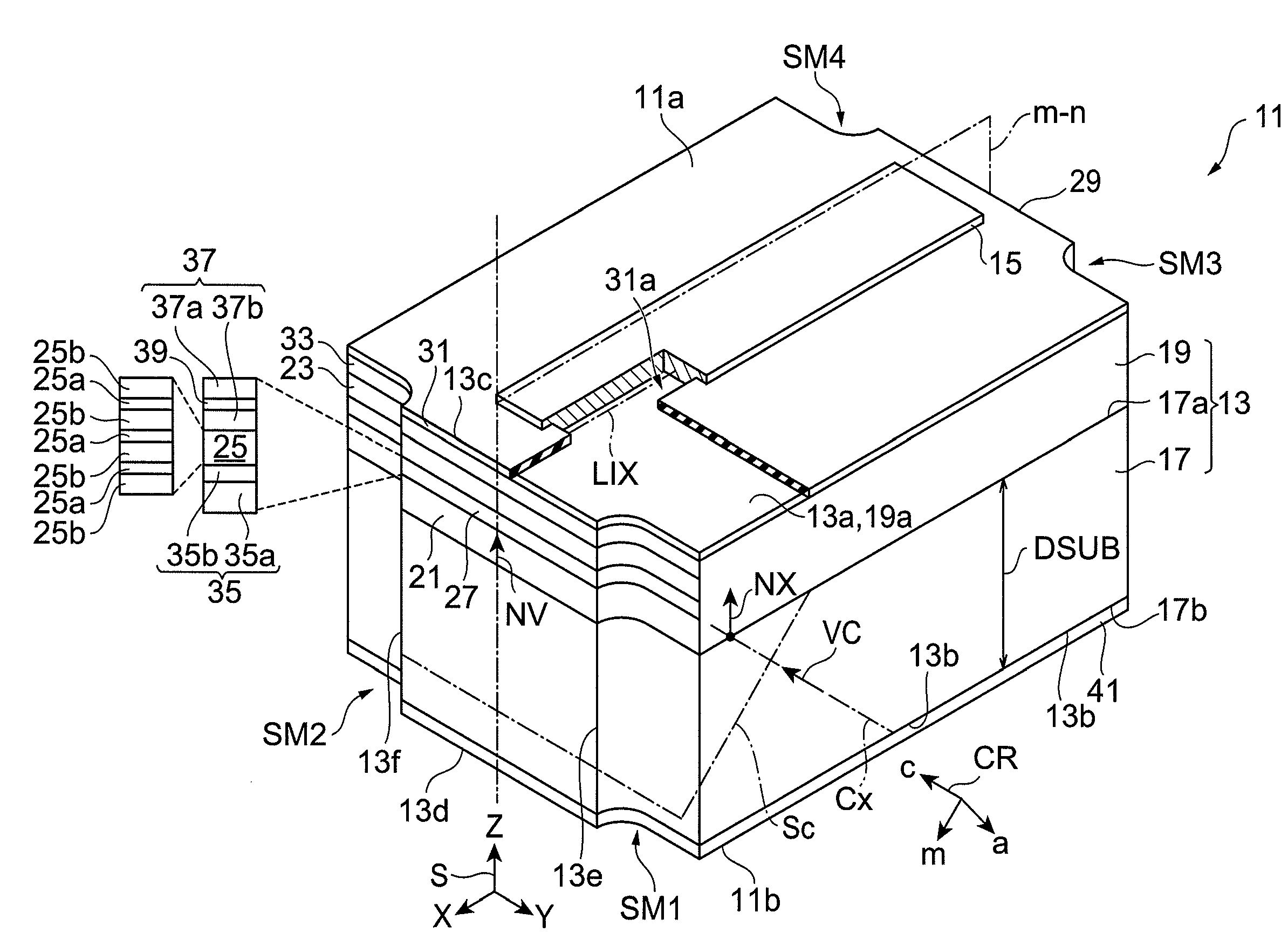
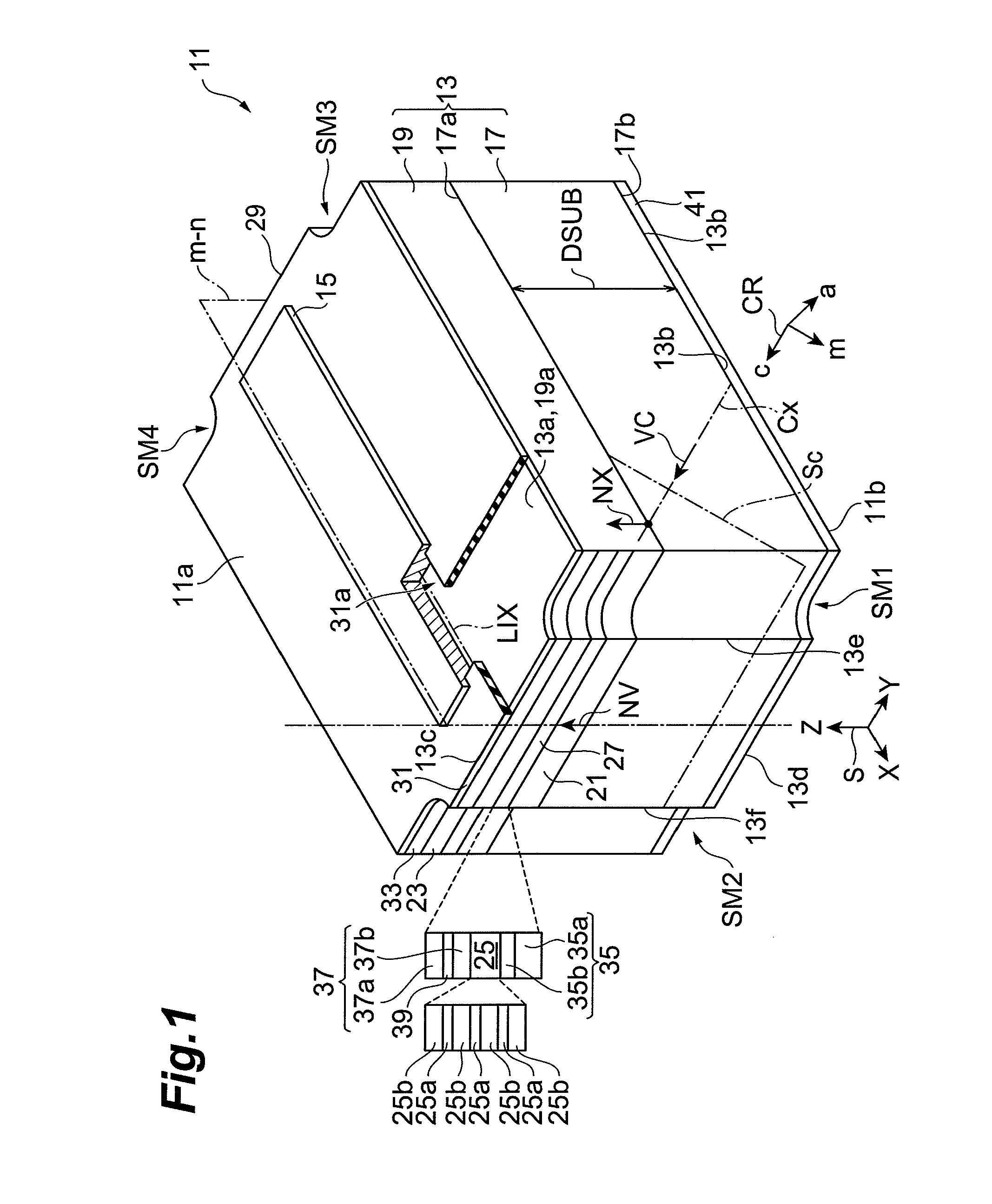
[0011]A group-III nitride semiconductor laser device according to an aspect of the present invention comprises: (a) a laser structure including a support base and a semiconductor region, the support base comprising a hexagonal group-III nitride semiconductor and having a semipolar principal surface, and the semiconductor region being provided on the semipolar principal surface of the support base; and (b) an electrode being provided on the semiconductor region of the laser structure, the semiconductor region including a first cladding layer of a first conductivity type gallium nitride-based semiconductor, a second cladding layer of a second conductivity type gallium nitride-based semiconductor, and an active layer, the active layer being provided between the first cladding layer and the second cladding layer, the first cladding layer, the second cladding layer, and the active layer being arranged along a normal axis to the semipolar principal surface, the active layer including a gallium nitride-based semiconductor layer, a c-axis of the hexagonal group-III nitride semiconductor of the support base tilting at a finite angle ALPHA with respect to the normal axis toward an m-axis of the hexagonal group-III nitride semiconductor, the angle ALPHA being in a range of not less than 45° and not more than 80° or in a range of not less than 100° and not more than 135°, the laser structure comprising first and second fractured faces, the first and second fractured faces intersecting with an m-n plane defined by the m-axis of the hexagonal group-III nitride semiconductor and the normal axis, a laser cavity of the group-III nitride semiconductor laser device including the first and second fractured faces, the laser structure including first and second surfaces, the second surface being opposite to the first surface, the semiconductor region being located between the first surface and the support base, each of the first and second fractured faces extending from an edge of the first surface to an edge of the second surface, the laser structure having a scribed mark, the scribed mark extending from the edge of the first surface to the edge of the second surface, at one end of the first fractured face, and the scribed mark having a depressed shape, the depressed shape extending from the edge of the first surface to the edge of the second surface. In this group-III nitride semiconductor laser device, since the fractured face is provided along the scribed mark of the depressed shape extending from the edge of the first surface to the edge of the second surface at one end of the first fractured face, the fractured face is expected to have sufficient perpendicularity and flatness, and thus, the fractured face can have the perpendicularity and flatness enough for a laser cavity mirror. Therefore, it is feasible to provide the group-III nitride semiconductor laser device with the laser cavity enabling a low threshold current.
[0027]In this method for fabricating the group-III nitride semiconductor laser device, the scribed through-holes are formed by laser irradiation to the first surface or the second surface of the laser structure, using a laser scriber. According to this method, the laser may be applied to either the first surface or the second surface. Particularly, when the laser is applied to the second surface, damages and debris of an epitaxially grown surface (epitaxial surface) are reduced.

Problems solved by technology

However, this orientation of the laser waveguide does not allow use of the conventional cleaved facets such as c-planes, a-planes, or m-planes for the laser cavity mirrors.
It becomes a heavy burden to find process conditions for obtaining excellent dry-etched faces in the current technical level.

Method used


Image

  • Group-III nitride semiconductor laser device, and method for fabricating group-III nitride semiconductor laser device
  • Group-III nitride semiconductor laser device, and method for fabricating group-III nitride semiconductor laser device
  • Group-III nitride semiconductor laser device, and method for fabricating group-III nitride semiconductor laser device

Examples


example

[0085]A laser diode shown in FIG. 7 is grown by organometallic vapor phase epitaxy as described below. The raw materials used are as follows: trimethyl gallium (TMGa); trimethyl aluminum (TMAl); trimethyl indium (TMIn); ammonia (NH3); and silane (SiH4). A substrate 71 is prepared. A GaN substrate is prepared as the substrate 71, and the GaN substrate is cut with a wafer slicing apparatus at an angle in a range of 0° to 90° to the m-axis from a (0001) GaN ingot thickly grown by HVPE, in such a manner that the angle ALPHA of the c-axis tilted toward the m-axis has a desired off angle in a range of 0° to 90°. For example, when the substrate is formed by cutting at the angle of 75°, the resultant substrate is prepared as a GaN substrate having a {20-21}-plane.

[0086]Before the growth, the substrate is observed by the cathodoluminescence method in order to estimate the stacking fault density of the substrate. In the cathodoluminescence, an emission process of carriers excited by an electr...


PUM


Abstract

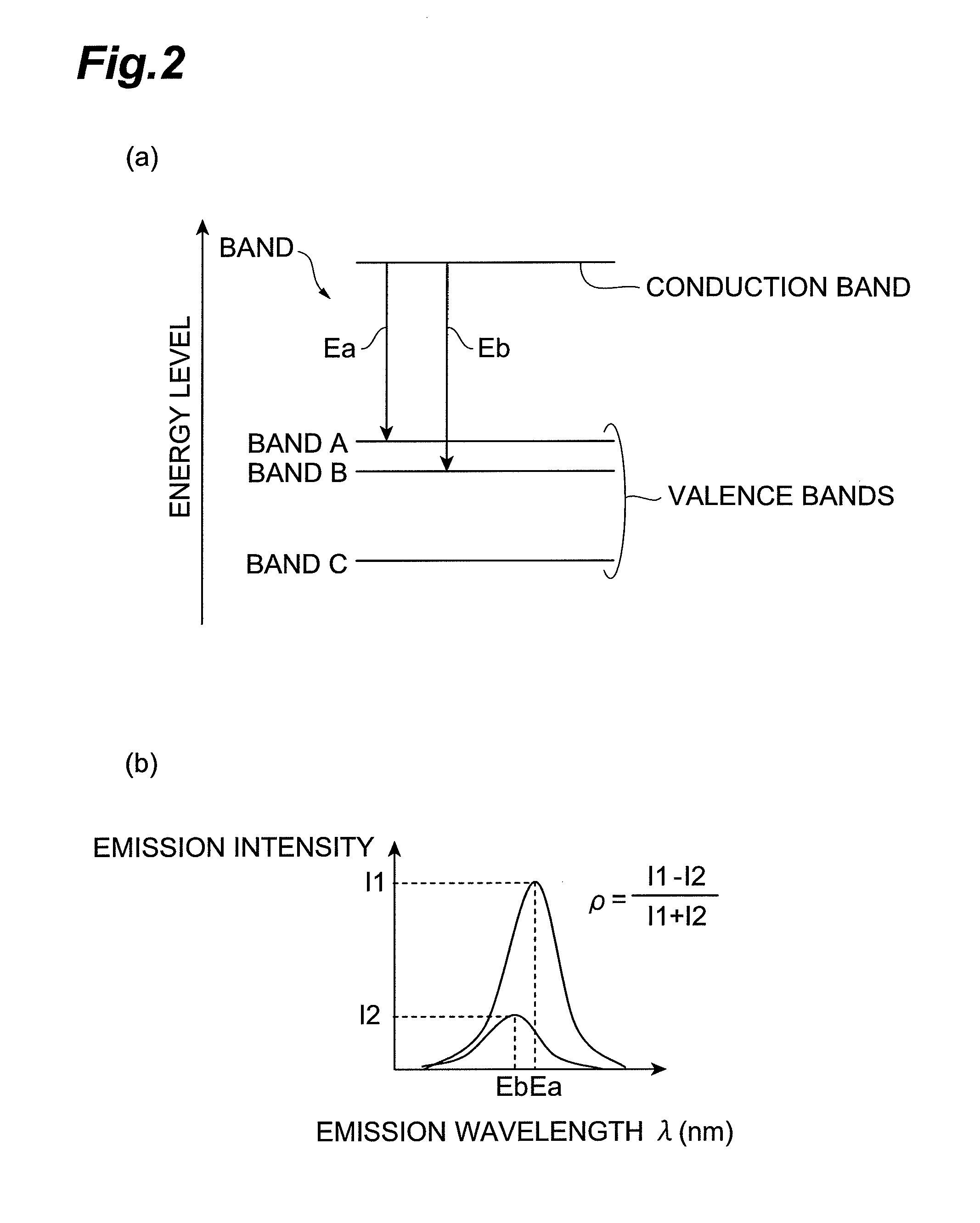
Provided is a group-III nitride semiconductor laser device with a laser cavity enabling a low threshold current, on a semipolar surface of a support base the c-axis of a hexagonal group-III nitride of which tilts toward the m-axis. In a laser structure 13, a first surface 13a is a surface opposite to a second surface 13b and first and second fractured faces 27, 29 extend each from an edge 13c of the first surface 13a to an edge 13d of the second surface 13b. A scribed mark SM1 extending from the edge 13c to the edge 13d is made, for example, at one end of the first fractured face 27, and the scribed mark SM1 or the like has a depressed shape extending from the edge 13c to the edge 13d. The fractured faces 27, 29 are not formed by dry etching and thus are different from the conventional cleaved facets such as c-planes, m-planes, or a-planes. It is feasible to use emission of a band transition enabling a low threshold current.

Description

BACKGROUND OF THE INVENTION[0001]1. Field of the Invention[0002]The present invention relates to a group-III nitride semiconductor laser device, and a method for fabricating the group-III nitride semiconductor laser device.[0003]2. Related Background Art[0004]Non-patent Document 1 (Jpn. J. Appl. Phys. Vol. 35, (1996) L74-L76) describes a semiconductor laser made on a c-plane sapphire substrate. The mirror faces of the semiconductor laser are formed by dry etching. The Document 1 shows micrographs of the laser cavity mirror faces of the laser, and describes that the roughness of the end faces is about 50 nm.[0005]Non-patent Document 2 (Appl. Phys. Express 1 (2008) 091102) describes a semiconductor laser formed on a (11-22) plane GaN substrate. The mirror faces of the semiconductor laser are formed by dry etching.[0006]Non-patent Document 3 (Jpn. J. Appl. Phys. Vol. 46, (2007) L789) describes a gallium nitride (GaN)-based semiconductor laser. It proposes generation of laser light pola...

Claims


Application Information

Patent Timeline
Patent Type & Authority Patents(United States)
IPC IPC(8): H01L21/00
CPCB82Y20/00H01S5/34333H01S5/0202H01L21/02389H01L21/02433H01L21/02458H01L21/0254H01S5/0014H01S5/1082H01S5/3202H01S5/3211H01L21/0262H01S5/320275H01S5/10H01S5/30
Inventor TAKAGI, SHIMPEIYOSHIZUMI, YUSUKEKATAYAMA, KOJIUENO, MASAKIIKEGAMI, TAKATOSHI
Owner SUMITOMO ELECTRIC IND LTD
Learn More