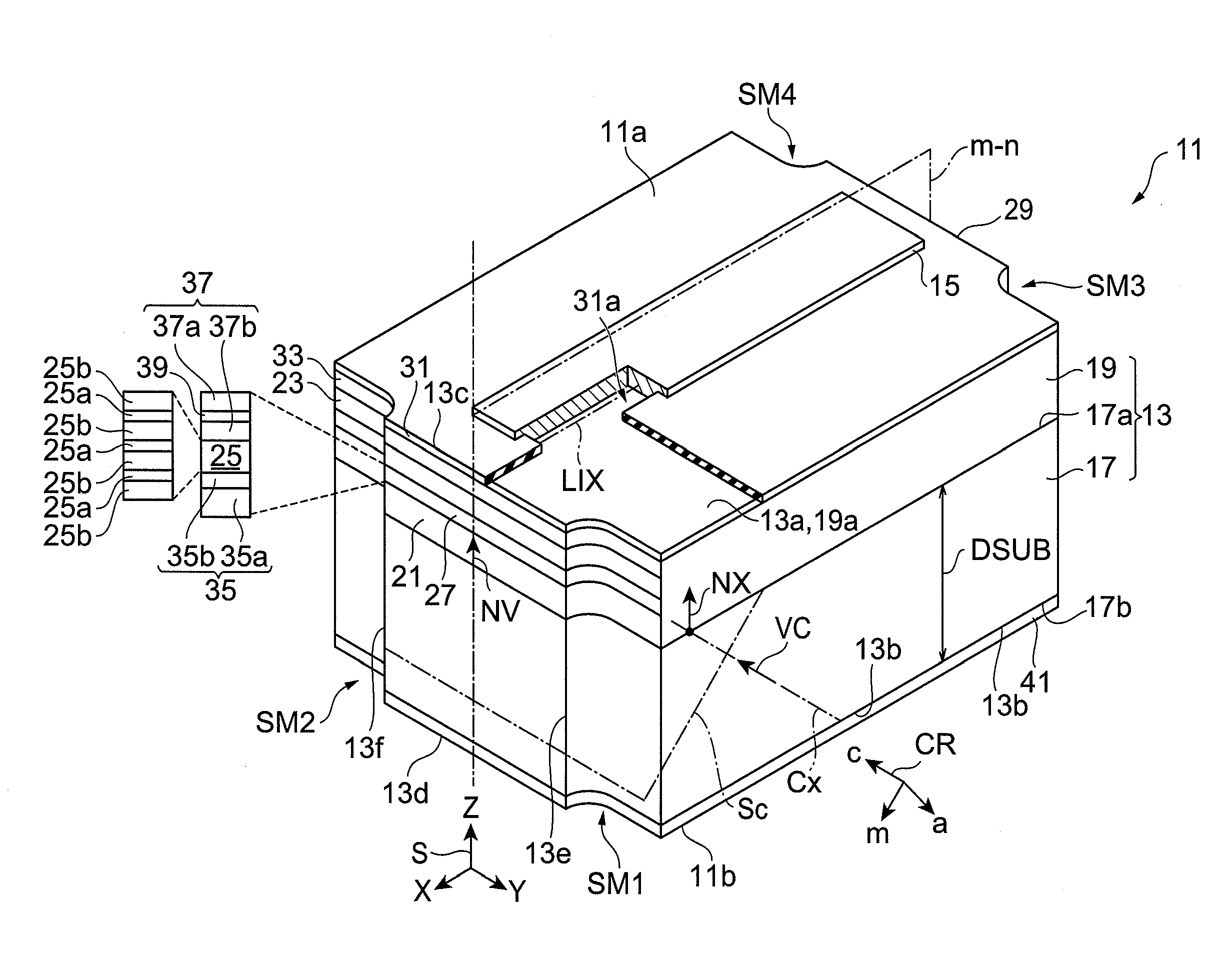
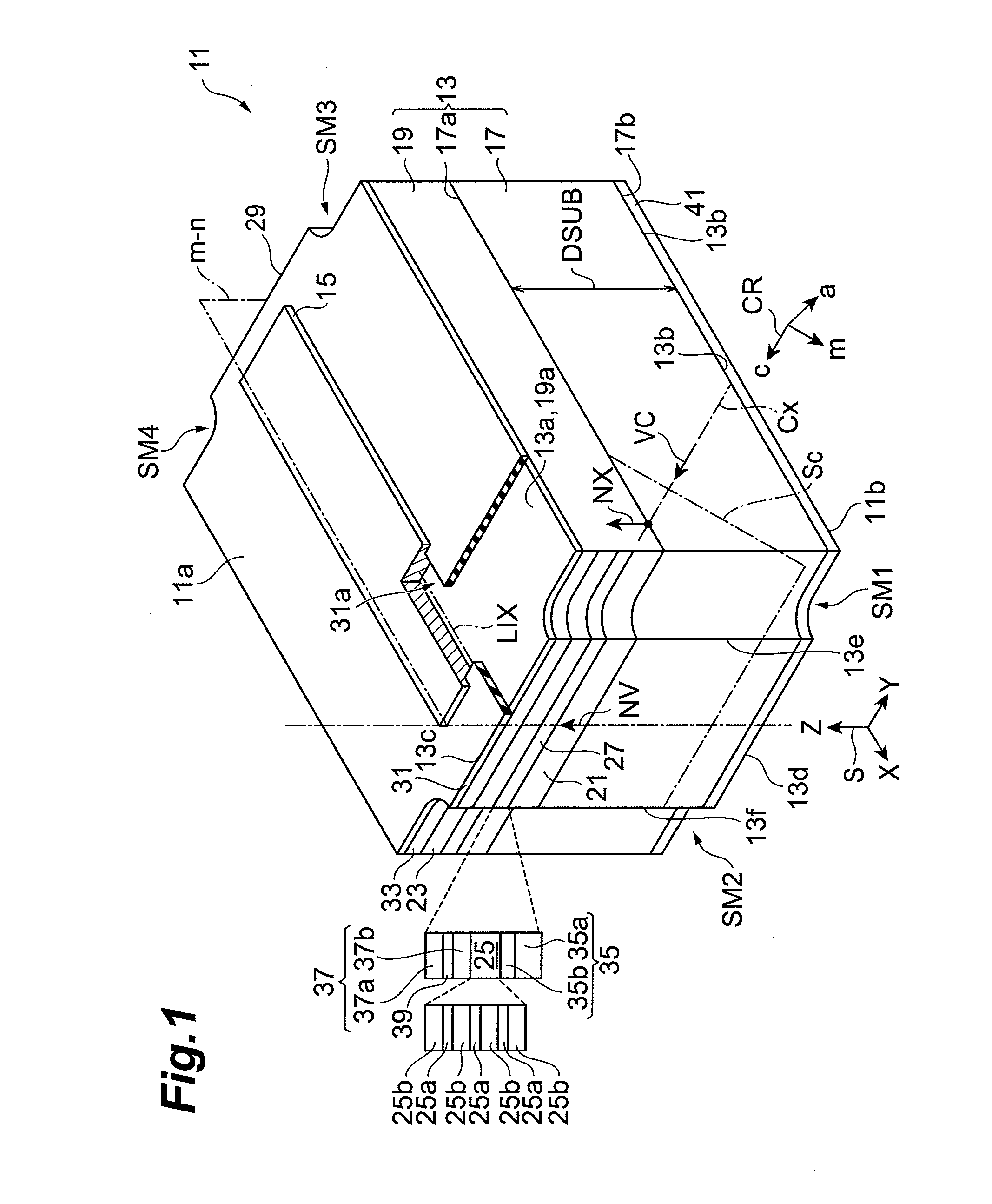
[0011]A group-III nitride semiconductor laser device according to an aspect of the present invention comprises: (a) a laser structure including a support base and a semiconductor region, the support base comprising a hexagonal group-III nitride semiconductor and having a semipolar principal surface, and the semiconductor region being provided on the semipolar principal surface of the support base; and (b) an
electrode being provided on the semiconductor region of the laser structure, the semiconductor region including a first cladding layer of a first
conductivity type
gallium nitride-based semiconductor, a second cladding layer of a second
conductivity type
gallium nitride-based semiconductor, and an
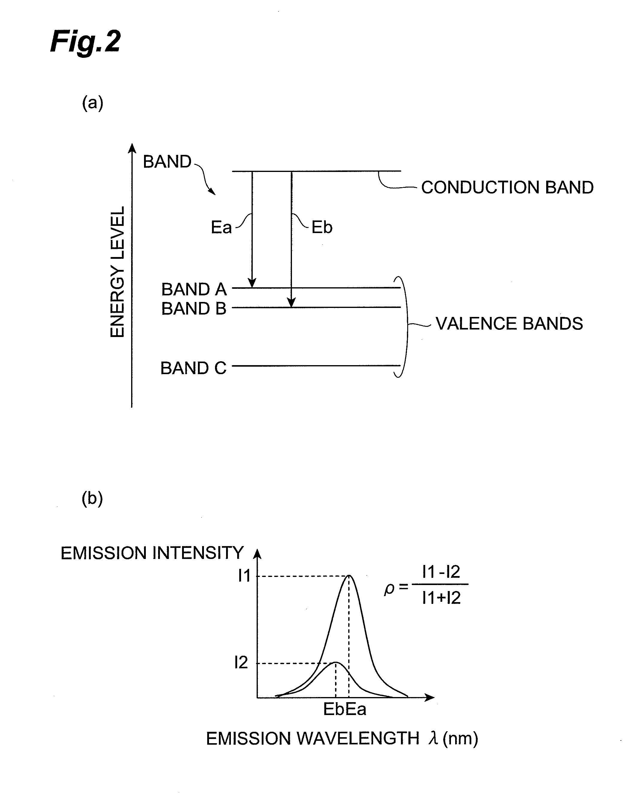
active layer, the
active layer being provided between the first cladding layer and the second cladding layer, the first cladding layer, the second cladding layer, and the
active layer being arranged along a normal axis to the semipolar principal surface, the active layer including a
gallium nitride-based semiconductor layer, a c-axis of the hexagonal group-III nitride semiconductor of the support base tilting at a finite
angle ALPHA with respect to the normal axis toward an m-axis of the hexagonal group-III nitride semiconductor, the
angle ALPHA being in a range of not less than 45° and not more than 80° or in a range of not less than 100° and not more than 135°, the laser structure comprising first and second fractured faces, the first and second fractured faces intersecting with an m-n plane defined by the m-axis of the hexagonal group-III nitride semiconductor and the normal axis, a laser cavity of the group-III nitride semiconductor laser device including the first and second fractured faces, the laser structure including first and second surfaces, the second surface being opposite to the first surface, the semiconductor region being located between the first surface and the support base, each of the first and second fractured faces extending from an edge of the first surface to an edge of the second surface, the laser structure having a scribed mark, the scribed mark extending from the edge of the first surface to the edge of the second surface, at one end of the first fractured face, and the scribed mark having a depressed shape, the depressed shape extending from the edge of the first surface to the edge of the second surface. In this group-III nitride semiconductor laser device, since the fractured face is provided along the scribed mark of the depressed shape extending from the edge of the first surface to the edge of the second surface at one end of the first fractured face, the fractured face is expected to have sufficient perpendicularity and flatness, and thus, the fractured face can have the perpendicularity and flatness enough for a laser cavity mirror. Therefore, it is feasible to provide the group-III nitride semiconductor laser device with the laser cavity enabling a low
threshold current.
[0027]In this method for fabricating the group-III nitride semiconductor laser device, the scribed through-holes are formed by laser
irradiation to the first surface or the second surface of the laser structure, using a laser
scriber. According to this method, the laser may be applied to either the first surface or the second surface. Particularly, when the laser is applied to the second surface, damages and debris of an epitaxially grown surface (epitaxial surface) are reduced.

