Manufacturing method of semiconductor device

a manufacturing method and semiconductor technology, applied in the direction of electrical appliances, decorative surface effects, decorative arts, etc., can solve the problems of high accuracy, thickness of etching masks, and difficulty in forming fine resist patterns by lithography, so as to reduce the roughness of the pattern and reduce the deterioration of the processed configuration

Active Publication Date: 2012-01-10
RENESAS ELECTRONICS CORP
View PDF9 Cites 28 Cited by
  • Summary
  • Abstract
  • Description
  • Claims
  • Application Information

AI Technical Summary

Benefits of technology

[0015]It is an object of the present invention to provide a manufacturing method of a semiconductor device that reduces the deterioration in processed configuration and the pattern roughness of a film to be processed, sticks closely to its original design and can be applied to a dual damascene process and the like.
[0017]According to the manufacturing method of the semiconductor device in the present invention, since the hardening treatment is performed for at least one processing mask layer, the deterioration in processed configuration and the pattern roughness of the film to be processed can be reduced and the pattern sticks closely to its original design.
[0019]According to another manufacturing method of the semiconductor device in the present invention, when the dual damascene structure is formed, the etching resistance can be raised only at the part from the surface to the necessary depth point, and the part buried in the via hole is made not to be affected by the hardening treatment.

Problems solved by technology

Recently, with the demands for miniaturization and high accuracy of a semiconductor device, it is a very important technical development issue to realize that a fine resist pattern is formed by lithography with high accuracy and a film to be processed is dry etched with high accuracy using the resist pattern as an etching mask at a fine processing step in its manufacturing process.
Secondly, it is necessary to sacrifice plasma dry etching resistance in order to improve the resolution of a resist material.
Firstly, the etching mask has to have thickness to endure the dry etching for the film to be processed.
According to the conventional method using a monolayer resist on the film to be processed as the etching mask, it is hard to implement that the fine resist pattern is formed by lithography with high accuracy and the film to be processed is dry etched using the resist pattern as the etching mask with high accuracy.
In this case, since the aspect ratio of the resist pattern is too high, the pattern collapse is generated in the formed resist pattern.
When the film thickness of the resist is reduced to 120 nm to prevent the pattern collapse of the resist pattern, the resist cannot serve as the mask of the dry etching and the film to be processed after etching chips off.
In other hardening treatments, similar pattern deformation is generated although its degree is different, which is a big problem in manufacturing the device.
That is, according to the above method, although the chipping off or LER of the film to be processed after etching can be improved, fidelity to the original design considerably deteriorates.
However, even in the multilayer resist method, although both lower layer and middle layer are required to be more rigid as the pattern becomes fine, sufficiently uniform rigidity is not always provided in the coating type film by the heat hardening treatment only and as a result, the LER deterioration is generated in the pattern after etching.
However, the problem in the multilayer hard mask method is that reflection coefficient control and chemical compatibility with the resist are bad.
In addition, when the multilayer hard mask method is applied to the via-first dual damascene step, although it is necessary to bury a lower-layer amorphous carbon (α-C layer) into a via hole, there is a problem in filling characteristics of the amorphous carbon.
In addition, although it is necessary to remove the buried amorphous silicon after the trench etching, since the amorphous carbon is rigid, it is difficult to remove it and as a result, the Low-k interlayer insulation film deteriorates (rise in k value).

Method used


Image

  • Manufacturing method of semiconductor device
  • Manufacturing method of semiconductor device
  • Manufacturing method of semiconductor device

Examples


first embodiment

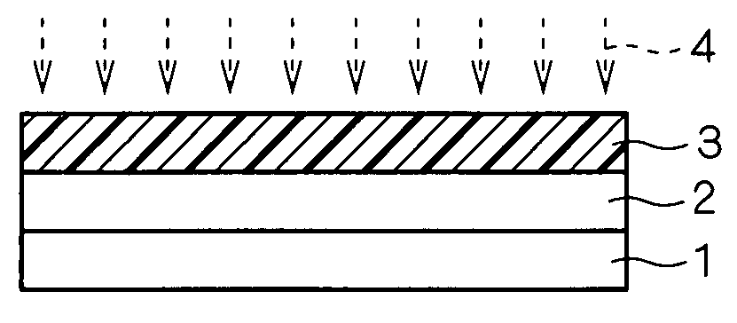
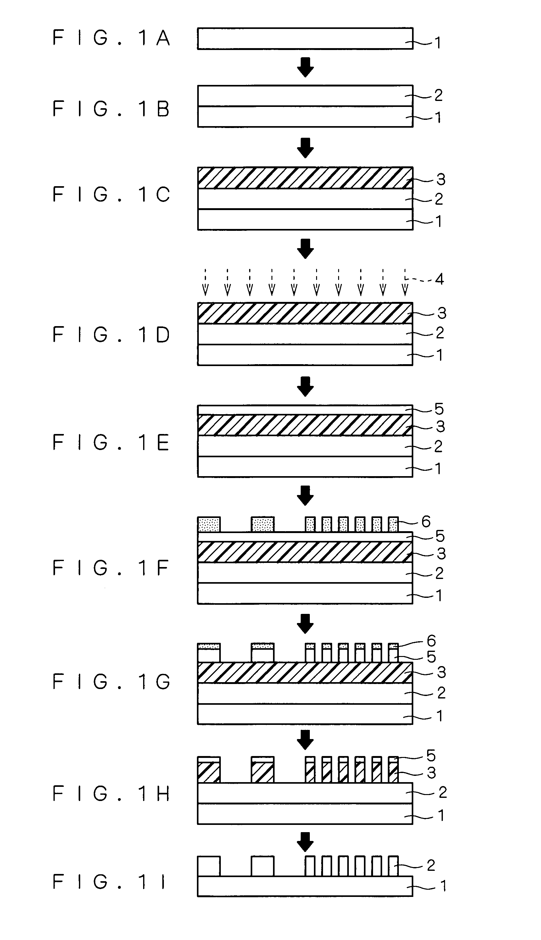
[0035]FIGS. 1A to 1I are flowcharts to explain a manufacturing method of a semiconductor device according to this embodiment. First, a film to be processed 2 is formed on a substrate 1 (Si substrate and the like) shown in FIG. 1A by sputtering, CVD (Chemical Vapor Deposition) and the like (FIG. 1B). In FIG. 1C, a coating type of lower organic film 3 having a film thickness of about 150 to 300 nm is applied to the film to be processed 2 and then a heat treatment is performed at 200 to 250° C. for about 1 to 1.5 minutes. By performing the heat treatment for the low organic film 3, a solvent can be sufficiently volatilized through a heat hardening process by a thermochemical reaction and a crosslink can be formed in a polymer by the reaction at a heat reaction active site.

[0036]In FIG. 1D, hardening treatment 4 is performed such that any one of Ar, B, As, P, C and H is implanted to the lower organic film 3 after the heat treatment and the lower organic film 3 is carbonized (graphitized...

second embodiment

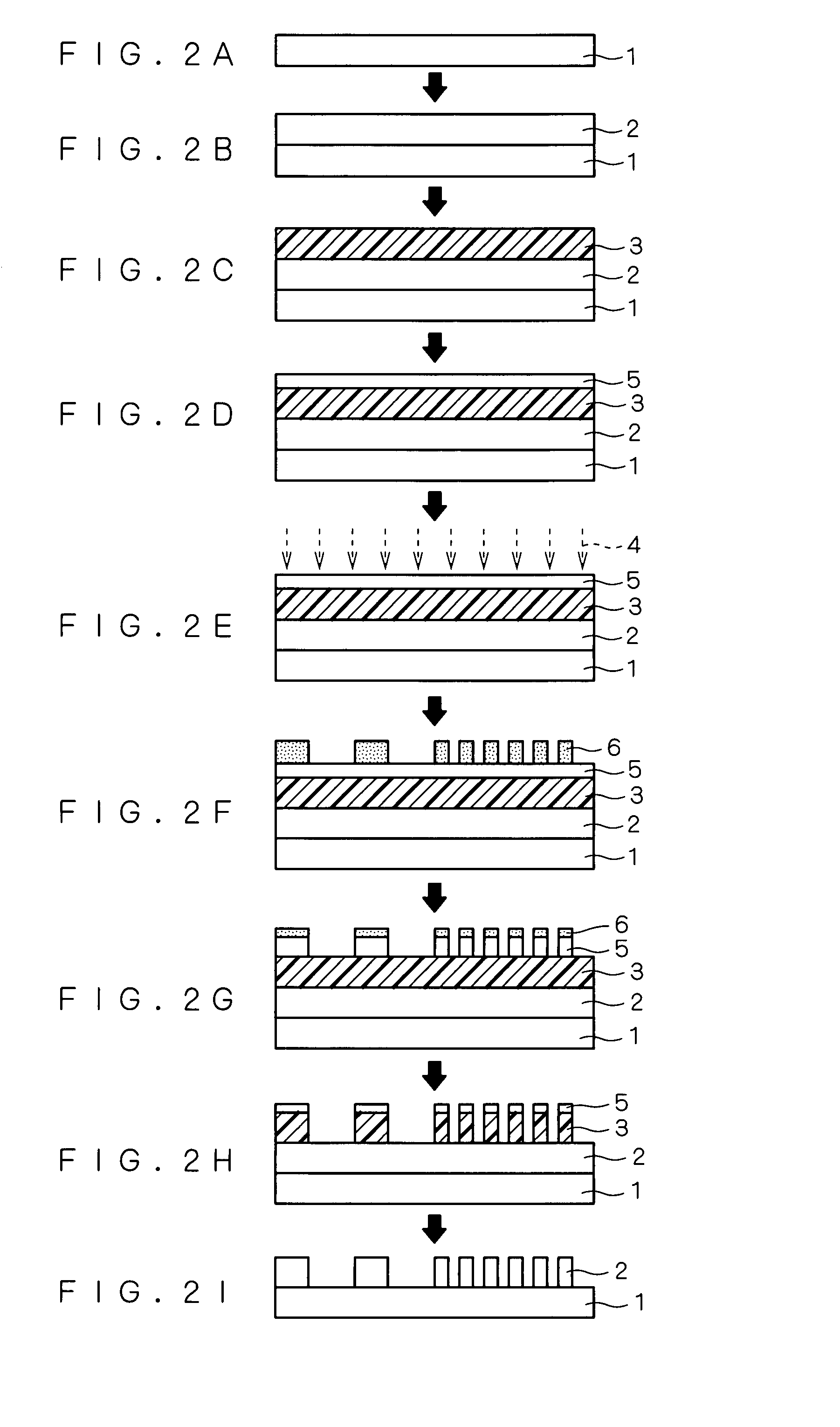
[0047]FIGS. 2A to 2I are flowcharts to explain a manufacturing method of a semiconductor device according to this embodiment. First, a film to be processed 2 is formed on a substrate 1 (Si substrate and the like) shown in FIG. 2A by sputtering, CVD and the like (FIG. 2B). In FIG. 2C, a coating type of lower organic film 3 having a film thickness of about 150 to 300 nm is applied to the film to be processed 2 and then a heat treatment is performed at 200 to 250° C. for about 1 to 1.5 minutes. By performing the heat treatment for the low organic film 3, a solvent can be sufficiently volatilized through a heat hardening process by a thermochemical reaction and a crosslink can be formed in a polymer by the reaction at a thermal reaction active site.

[0048]In FIG. 2D, a middle layer 5 is formed on the lower organic film 3 after the heat treatment. A silsesquioxane-type polymer such as inorganic SOG or organic SOG is used for the middle layer 5 and applied so as to have a thickness of abou...

third embodiment

[0060]FIGS. 3A to 3I are flowcharts to explain a manufacturing method of a semiconductor device according to this embodiment. First, a film to be processed 2 is formed on a substrate 1 (Si substrate and the like) shown in FIG. 3A by sputtering, CVD and the like (FIG. 3B). In FIG. 3C, a coating type of lower organic film 3 having a film thickness of about 150 to 300 nm is applied to the film to be processed 2 and then a heat treatment is performed at 200 to 250° C. for about 1 to 1.5 minutes. By performing the heat treatment for the low organic film 3, a solvent can be sufficiently volatilized through a heat hardening process by a thermochemical reaction and a crosslink can be formed in a polymer by the reaction at a thermal reaction active site.

[0061]In FIG. 3D, a hardening treatment is performed such that any one of Ar, B, As, P, C and H is implanted to the lower organic film 3 after the heat treatment and the lower organic film 3 is carbonized (graphitized). In addition, instead o...


PUM

PropertyMeasurementUnit
thicknessaaaaaaaaaa
thicknessaaaaaaaaaa
thicknessaaaaaaaaaa

Abstract

It is an object of the present invention to provide a method of manufacturing a semiconductor device that reduces the deterioration in processed configuration and the pattern roughness of a film to be processed, and is close to the original design and applicable to a dual damascene step and the like. The manufacturing method comprises a processing mask layer forming step of forming a processing mask layer (a lower organic film and a middle layer) comprising at least one film, and hardening treatment for at least one film of the processing mask layer by applying a film and heat hardening treatment; a processing mask layer etching step of applying a resist film for exposure to the processing mask layer, exposing and developing it to form a resist pattern, and etching the processing mask layer using the resist pattern as a mask; and a film to be processed etching step of etching the film to be processed using the pattern of the processing mask layer formed at the processing mask layer etching step as a mask.

Description

BACKGROUND OF THE INVENTION[0001]1. Field of the Invention[0002]The present invention relates to a manufacturing method of a semiconductor device and more particularly, to a manufacturing method of a semiconductor device in which a predetermined pattern is formed in a film to be processed using a multilayer film.[0003]2. Description of the Background Art[0004]Recently, with the demands for miniaturization and high accuracy of a semiconductor device, it is a very important technical development issue to realize that a fine resist pattern is formed by lithography with high accuracy and a film to be processed is dry etched with high accuracy using the resist pattern as an etching mask at a fine processing step in its manufacturing process.[0005]There are three restrictions mainly in forming the fine resist pattern by lithography as follows. Firstly, it is necessary to thin the resist as much as possible to improve resolution and prevent the pattern from being destroyed. Secondly, it is...

Claims


Application Information

Patent Timeline
Patent Type & Authority Patents(United States)
IPC IPC(8): C03C15/00C03C25/68H01L21/461H01L21/302C23F1/00
CPCH01L21/0332H01L21/0337H01L21/31058H01L21/31144H01L21/31155H01L21/76808H01L21/76825H01L21/76826
Inventor ISHIBASHI, TAKEOYONEKURA, KAZUMASATADOKORO, MASAHIROYOSHIKAWA, KAZUNORIONO, YOSHIHARU
Owner RENESAS ELECTRONICS CORP
Why Eureka
Try Eureka