Arrangement for the illumination of a substrate with a plurality of individually shaped particle beams for high-resolution lithography of structure patterns

a technology of structure pattern and arrangement, which is applied in the direction of cathode ray tubes/electron beam tubes, electrical equipment, etc., can solve the problems of reducing the productivity of high-resolution electron beam writers in high-end mask fabrication, increasing writing times, and sacrificing a, so as to achieve high substrate throughput and achieve the effect of reducing the flexibility of structure patterns, and reducing the number of lithography errors

Active Publication Date: 2012-04-03
VISTEC ELECTRON BEAM
View PDF33 Cites 16 Cited by
  • Summary
  • Abstract
  • Description
  • Claims
  • Application Information

AI Technical Summary

Benefits of technology

[0017]It is the object of the invention to find a novel possibility for illuminating a substrate with a plurality of individually shaped, controllable particle beams which permits a high-resolution structuring of substrates with a high substrate throughput without limiting the flexibility of the structure patterns to be illuminated or sacrificing a high substrate throughput for a high flexibility of structure patterns to be illuminated.
[0030]It has proven advantageous to arrange the pairs of electrodes of the deflector cell array of every multibeam deflector array orthogonal to one another on the deflector chips located one on top of the other.
[0035]To increase the flexibility of the exposable structure patterns, at least the second multiple-format diaphragm array has, in addition, special characters (structure patterns) for exposing repetitive structures.
[0039]The inventive solution makes it possible to realize an illumination of a substrate with particle radiation which permits a high-resolution structuring of substrates with a high substrate throughput without limiting the flexibility of the structure patterns to be illuminated or sacrificing substrate throughput for a flexibility of the structure patterns that can be illuminated.

Problems solved by technology

Therefore, the image-generating methods for producing structures on masks and methods for direct structuring of wafers require increasingly longer writing times. Another reason for reduced productivity in high-resolution electron beam writers in high-end mask fabrication is the increasing degree of pre-distortion of the mask structure (optical proximity correction—OPC) to improve the structure resolution of high-productivity scanner objectives whose resolution, as is well-known, is diffraction-limited.
The demand in the semiconductor industry for lowering costs by reducing writing times in high-end mask fabrication and in direct exposure of wafers cannot be met by currently available single-beam writing technologies.
The disadvantages of these concepts are the high complexity of the beam modulators (thousands to hundreds of thousands of deflection systems / lenses) and the high data transfer rates owing to the fact that the circuit layout must be broken down into individual pixels without losses so that any hierarchy or compression is lost.
The drawbacks of this method consist in the fixed choice of character aperture geometry once it has been produced.
Another disadvantage of this exposure method consists in that, for reasons inherent to the principle, the current density within a character is constant.
Accordingly, a correction of the proximity effect depending on the exposure environment, particularly for a large character, is difficult to accomplish, which limits the usefulness and quality of the generated patterns.
A disadvantage in this method is the large amount of pixel data required for exposing a given pattern.
Further, a large number of complicated electrostatic correction elements such as lens arrays and deflection arrays are required for controlling the positions and focus planes of all of the partial beams in the target.
Another disadvantage in this method is that the individual beams in the target plane have the same size and are located on a fixed position grid.
In order to meet current requirements for positioning accuracy of patterns to be exposed (placement 2-5 nm), multiple exposures must be carried out with a slight positional offset (so-called grayscale exposure or gray beaming) which, as is well known, results in a deterioration of structure edges and reduces productivity.
A disadvantage in this method is the 1:1 imaging of the beam-shaping diaphragms in the target plane.
Accordingly, the quality of the diaphragms to be used would have to be even better, which appears very difficult in terms of technology, particularly with respect to the generation of such small corner radii.
Contamination effects at the diaphragm edges in practical operation are likewise effective in a ratio of 1:1 during exposure and therefore limit the quality of the patterns and the life of the diaphragms.
Further, the resources required for providing an entire array of radiation sources and for monitoring them individually is disadvantageous.
Further, it remains unclear how collective focusing is to be carried out when the target (e.g., machined wafer) has inevitable residual unevenness.
Finally, the collective deflection of all of the beams in the target plane presents a severe limitation on the quantity of beams that can be used simultaneously for exposure or defines a fixed grid for pattern generation.
In the case of very precise draft grids of the patterns, this substantially limits productivity and / or flexibility of the exposure device.
This concept has the disadvantage that the deflection of the beam bundles in two orthogonal directions is carried out in only one plane because, in deflection arrangements with such close proximity of the beams, simultaneous deflection in two orthogonal directions leads to large deflection errors which impair the edge quality and uniformity of the illumination.
Further, there are no concrete proposals for preventing crosstalk between the adjacent deflection systems which are arranged within a very confined space in proximity to the beam for every beam of the multibeam system.
Another weakness in the concept is the use of a plurality of small variable beam cross sections of comparable size for the exposure process of an entire design layout.

Method used


Image

  • Arrangement for the illumination of a substrate with a plurality of individually shaped particle beams for high-resolution lithography of structure patterns
  • Arrangement for the illumination of a substrate with a plurality of individually shaped particle beams for high-resolution lithography of structure patterns
  • Arrangement for the illumination of a substrate with a plurality of individually shaped particle beams for high-resolution lithography of structure patterns

Examples


Embodiment Construction

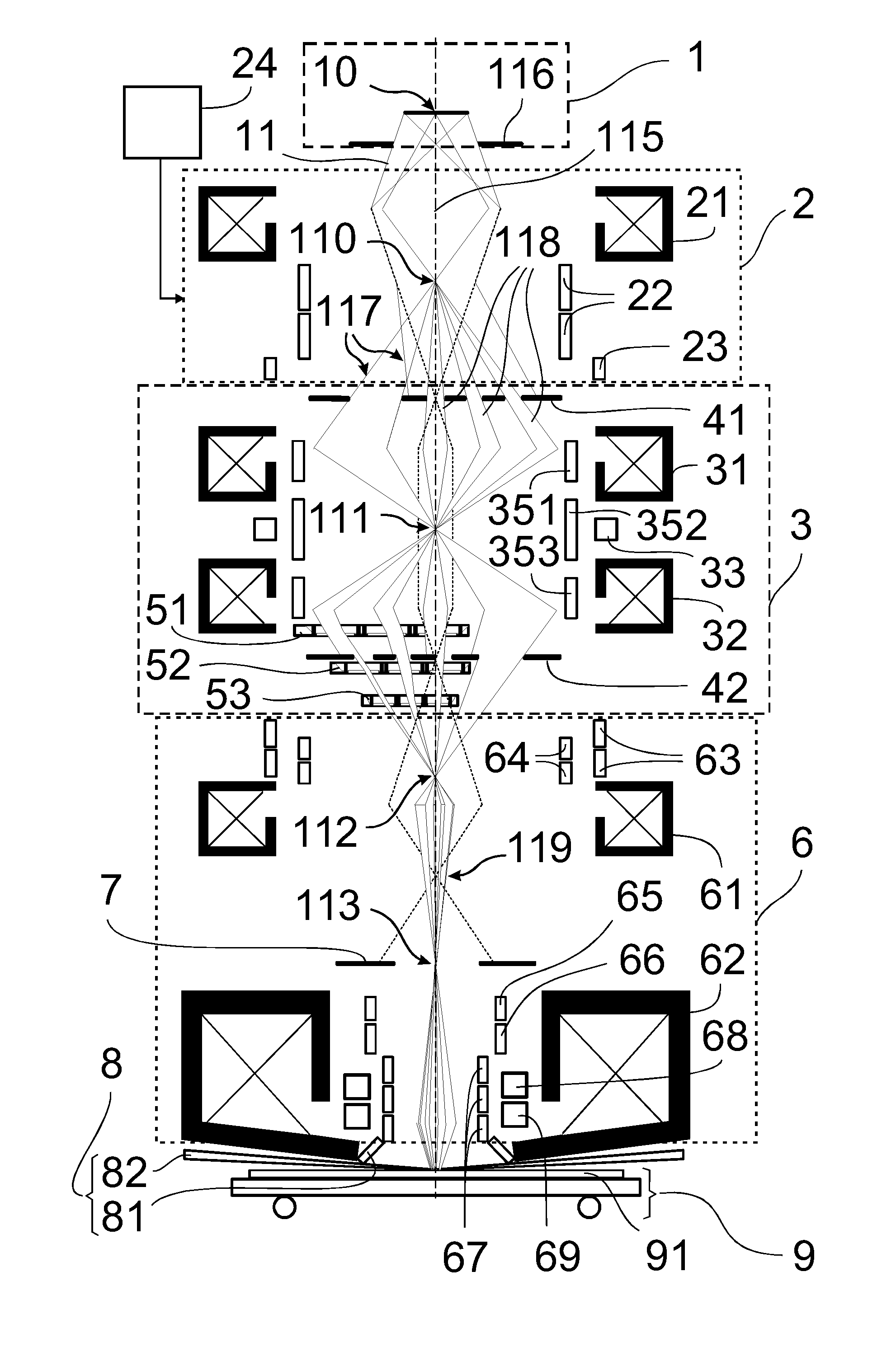
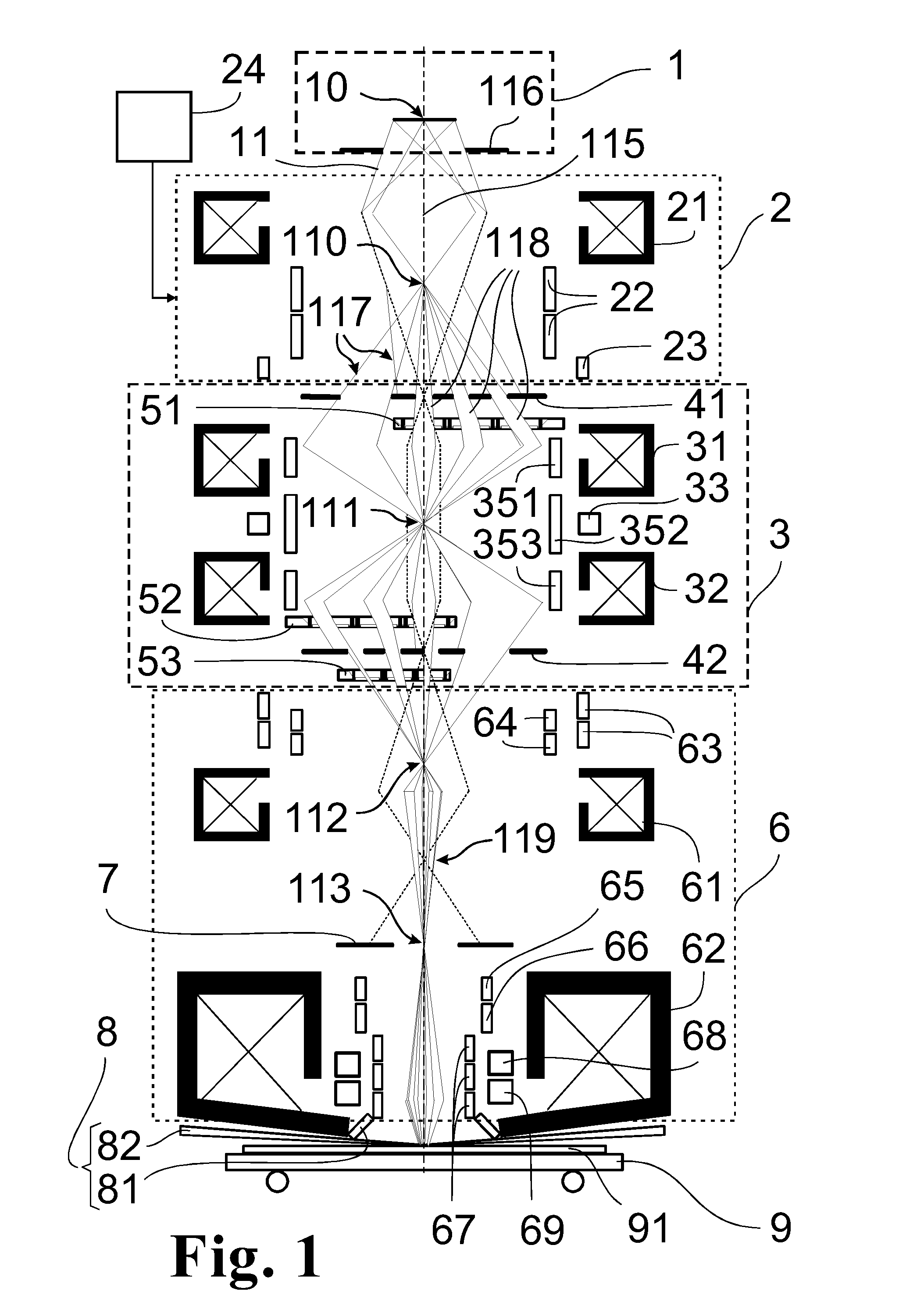
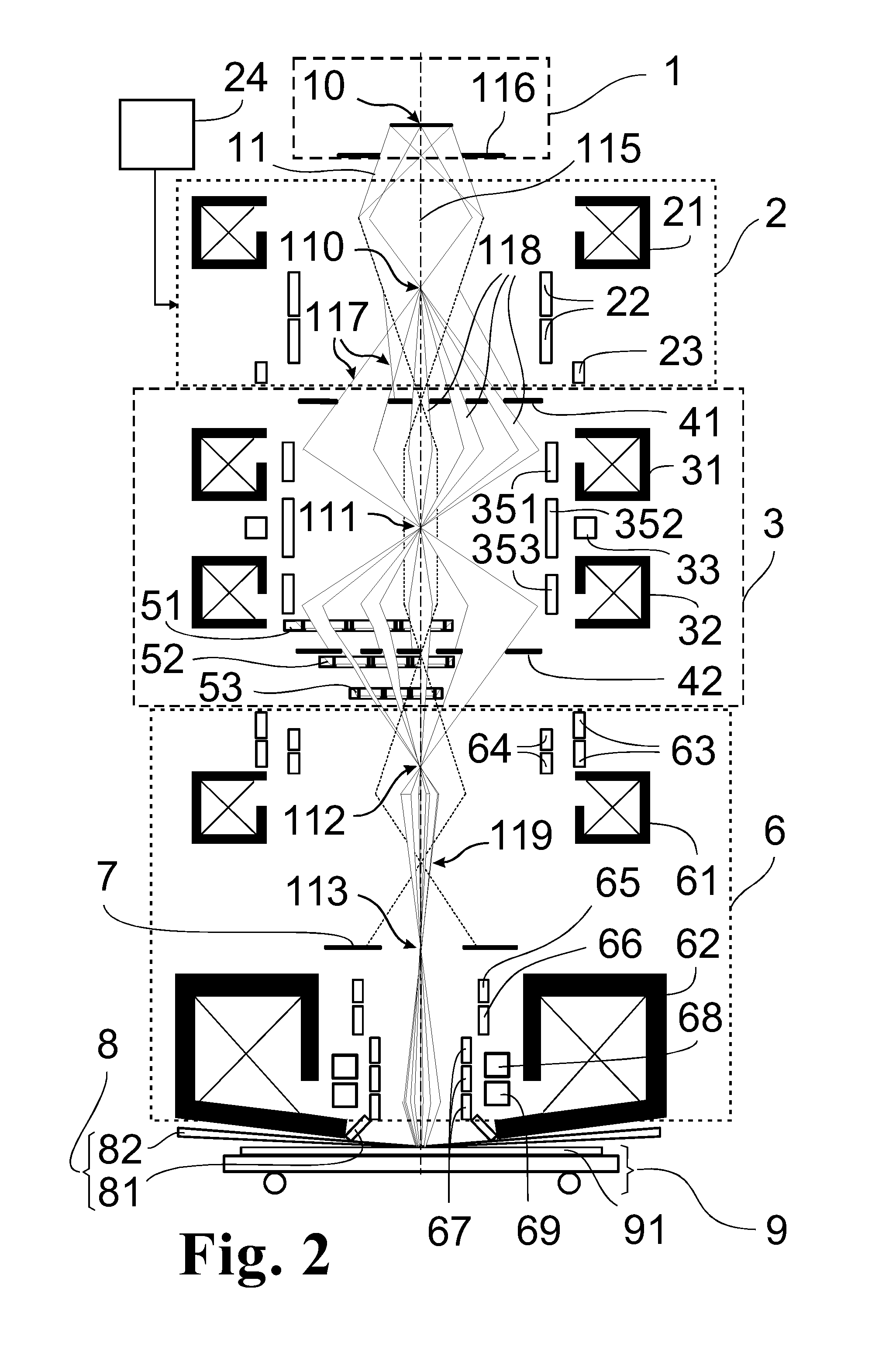
[0051]As is shown schematically in FIG. 1, the arrangement for substrate illumination with a plurality of individual particle beams basically comprises a particle beam source 1 defining an optical axis 115 along which the entire particle beam column up to the substrate 91 has the following components: an illumination system 2 for illuminating a first multiple-format diaphragm array 41 in selectable illumination groups, a beam modulator system 3 for generating a plurality of particle beamlets 118 containing, in addition to a condenser system 31-32, a group deflection system 35 and a multideflector system 5 cooperating with a multi-aperture diaphragm system 4 for individual deflection and shaping of the individual particle beamlets 118. Following the latter is a reduction system 6 for imaging the particle beamlets 118 transmitted by the multi-aperture diaphragm system 4 onto the substrate 91 moving on a substrate stage 9. A substrate monitoring sensor arrangement 8 is provided directl...


PUM

PropertyMeasurementUnit
edge lengthaaaaaaaaaa

Abstract

The invention is directed to an arrangement for the illumination of a substrate with a plurality of individually shaped, controllable particle beams, particularly for electron beam lithography in the semiconductor industry. It is the object of the invention to find a novel possibility for illuminating a substrate with a plurality of individually shaped, controllable particle beamlets which permits a high-resolution structuring of substrates with a high substrate throughput without limiting the flexibility of the applicable structure patterns or limiting the high substrate throughput due to a required flexibility.

Description

RELATED APPLICATIONS[0001]This application claims priority to German Patent Application No. DE 10 2008 062 450.0, filed Dec. 13, 2008, which is incorporated herein by reference in its entirety.FIELD OF THE INVENTION[0002]The invention is directed to an arrangement for the illumination of a substrate with a plurality of individually shaped, controllable particle beams with a particle beam source for emitting a particle beam, an illumination system for shaping and deflecting the particle beam for the illumination of a first aperture diaphragm array, wherein the aperture diaphragm array is a multiple-format diaphragm array for generating separate particle beamlets, a second multiple-format diaphragm array on which the first multiple-format diaphragm array is imaged by means of a condenser lens system and which has diaphragm apertures that are adapted to the first multiple-diaphragm array while taking into account the imaging scale, a multibeam deflector system for individual beam defle...

Claims


Application Information

Patent Timeline
Patent Type & Authority Patents(United States)
IPC IPC(8): G03F7/00H01J37/147H01J29/00G21K5/04
CPCB82Y10/00B82Y40/00G03F1/78G03F7/2063H01J37/045H01J37/09H01J37/1471H01J37/302H01J37/3174H01J37/3177H01J2237/0435H01J2237/045H01J2237/0492
Inventor DOERING, HANS-JOACHIMELSTER, THOMASHEINITZ, JOACHIMSLODOWSKI, MATTHIAS
Owner VISTEC ELECTRON BEAM
Why Eureka
Try Eureka