Low profile Schottky barrier diode for solar cells and solar panels and method of fabrication thereof

a technology of which is applied in the field of low-profile schottky barrier diodes for solar cells and solar panels, can solve the problems of extremely low forward voltage compared to the existing diodes in commercial production, and the resistance of the substrate is extremely low by a factor of ten, so as to reduce the cost of labor, eliminate the cost of packaging, and reduce the effect of reverse voltage leakag

Inactive Publication Date: 2012-04-24
TANIELIAN ARAM +1
View PDF14 Cites 13 Cited by
  • Summary
  • Abstract
  • Description
  • Claims
  • Application Information

AI Technical Summary

Benefits of technology

[0005]It is still further object of the invention to improve the reverse voltage breakdown to make it sharp in a typical Epi resistance and thickness at room and high temperatures.
[0006]It is yet another object of the invention to provide a tighter manufacturing tolerance for the series resistance of a Schottky barrier diode.
[0007]It is yet a further object of the invention to provide a Schottky barrier diode with a reduced parasitic action.
[0010]It is yet a further object of the invention to eliminate the packaging of a high power Schottky barrier diode in the implementation of the bypass diode in a solar panel, which reduces the cost of labor due to ease of assembly and eliminates a package cost.SUMMARY OF THE INVENTION
[0011]These and other objects, features and advantages of the invention are accomplished by the low profile Schottky barrier diode disclosed herein. To provide a low profile, thin Schottky diode, a Schottky diode of the present invention is constructed to have both an anode and a cathode on the same side of the diode, in which current direction is sideways in a very narrow gap of 3 to 6 microns between the anode and the cathode. In an embodiment of the present invention, a mesa-isolated Schottky barrier diode with a Zener structure formed on top of a very highly concentrated N++ substrate that has a resistivity of approximately 0.0001 ohm cm, and a fabrication method thereof are disclosed for generating a thin device having an anode and a cathode located on the same side of a chip. An epitaxial layer (Epi) lightly doped with an N-type dopant is located on a first surface of the substrate. A mesa is formed through the epitaxial layer on top of the substrate, and a Zener diode is formed in an annular region surrounding the mesa by P-type diffusion or implantation. The Epi thickness and concentration determine the Zener voltage breakdown. This Zener diode causes very low reverse voltage leakage and protects the Schottky barrier diode from high voltage spikes. A Schottky barrier contact is formed on the mesa and an ohmic contact is formed in a region outside the mesa on the first surface of the substrate. An anode electrode is connected to the Schottky barrier contact and a cathode electrode is connected to the ohmic contact. The Schottky barrier contact and the ohmic contact are formed by depositing a metal simultaneously in openings formed through an oxide layer that is grown on the surface of the mesa and on the remaining first surface of the substrate, in order to make a low series resistance connection to the Schottky barrier diode.
[0013]The resulting low profile Schottky barrier diode may be less than or equal to 1 mm in thickness with low leakage voltage breakdown at temperatures as high as 150° C. In particular, the Schottky barrier diode may have a thickness of 0.3 to 1 mm. Also, the substrate is extremely low in resistance by a factor of ten (10), which makes the forward voltage very low compared to the existing diode in commercial production. The mesa structure with an annular Zener diode at the periphery of the mesa gives a very sharp Zener breakdown, which will protect the Schottky barrier diode from being destroyed from voltage spike in the back bias mode in solar cells and panels.

Problems solved by technology

Also, the substrate is extremely low in resistance by a factor of ten (10), which makes the forward voltage very low compared to the existing diode in commercial production.

Method used


Image

  • Low profile Schottky barrier diode for solar cells and solar panels and method of fabrication thereof
  • Low profile Schottky barrier diode for solar cells and solar panels and method of fabrication thereof
  • Low profile Schottky barrier diode for solar cells and solar panels and method of fabrication thereof

Examples


Embodiment Construction

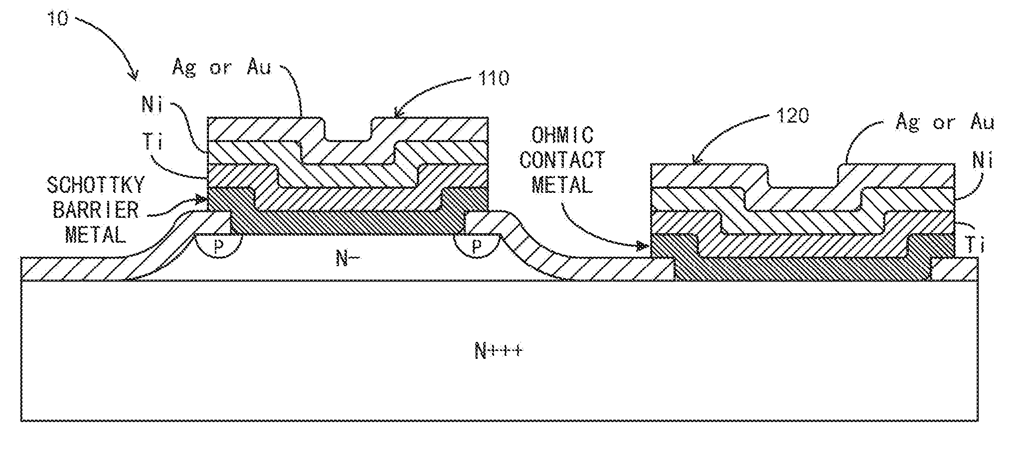
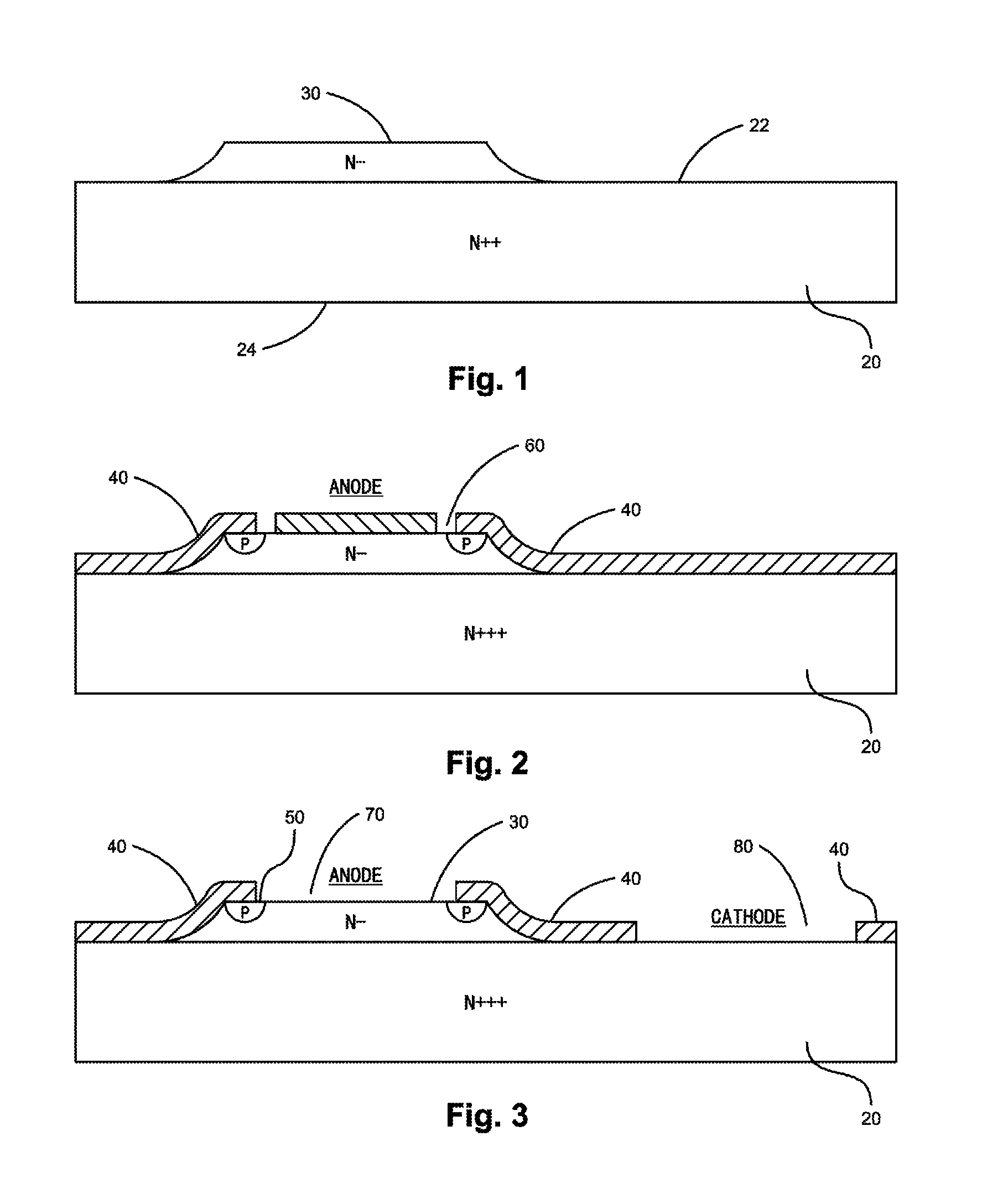
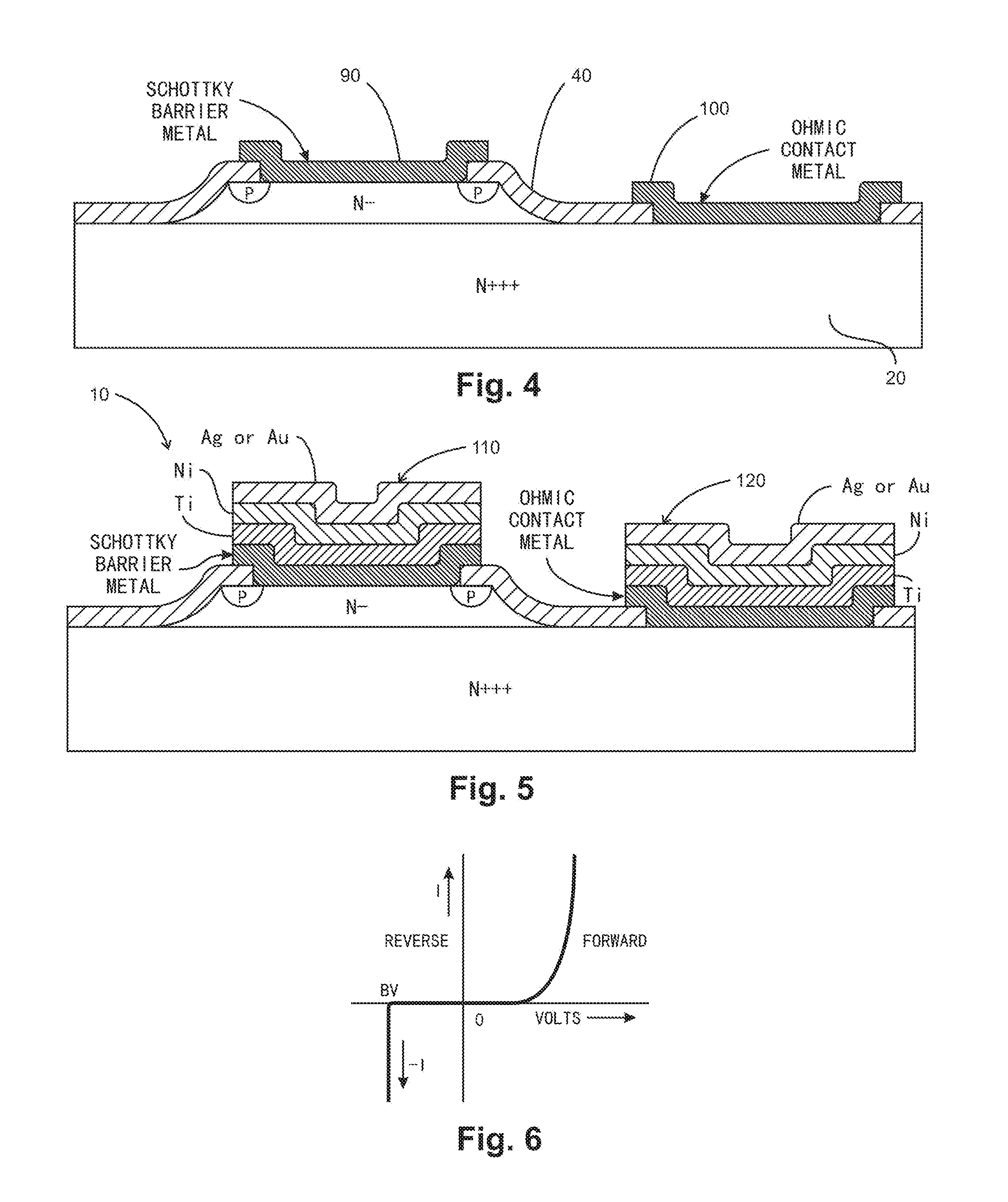
[0021]A mesa-isolated low profile Schottky barrier diode with an annular Zener diode with planar electrodes located on the same side of the diode and a method of fabrication thereof are disclosed for generating a low profile bypass diode device having a rugged structure.

[0022]FIG. 5 shows an embodiment of a Schottky barrier diode of the present invention. The Schottky barrier diode 10 comprises a substrate 20, a mesa 30 that is an epitaxial layer formed on the substrate 20, a Schottky barrier contact 90, an ohmic contact 100, an anode electrode 110, and a cathode electrode 120. The substrate 20 includes a first surface 22 and a second surface 24. The second surface 24 of the substrate is opposite to the first surface 22. The mesa 30 is located on a first portion of the first surface 22 of the substrate 20. The Schottky barrier contact 90 is formed on the mesa 30, and the ohmic contact 100 is formed on a second portion of the first surface 22 of the substrate 20. The second portion o...


PUM


Abstract

A low profile high power Schottky barrier bypass diode for solar cells and panels with the cathode and anode electrodes on the same side of the diode and a method of fabrication thereof are disclosed for generating a thin chip with both electrodes being on the same side of the chip. In an embodiment, a mesa isolation with a Zener diode over the annular region surrounding the central region of the mesa anode in the Epi of the substrate is formed. In an embodiment, a P-type Boron dopant layer is ion implanted in the annular region for the Zener Diode. This controls recovery from high voltage spikes from the diode rated voltage. A Schottky barrier contact for the anode and a contact for the cathode are simultaneously created on the same side of the chip.

Description

FIELD OF THE INVENTION[0001]The invention herein relates to semiconductor devices and methods relating thereto, and more particularly relates to improvement in Schottky diode devices.BACKGROUND OF THE INVENTION[0002]In the implementation of solar panels, it is desirable to use high power low Vf bypass Schottky diode for a multi-junction solar cell, silicon solar cell and thin film solar panels to prevent the solar cell from degrading due to hot spot. Such degrading occurs in a typical Schottky diode in the art, which has an anode on the top of the diode and a cathode at the bottom of the diode. In the structure of the typical Schottky diode, current flows from the top to the bottom vertically and the flow path is long due to the thicknesses of an epitaxial layer (Epi) and of a substrate and resistance of the substrate. Also, the diode will be thick when sandwiched between electrodes in a panel, which in turn will make the panel thicker than desired. A desired way is to make the pane...

Claims


Application Information

Patent Timeline
Patent Type & Authority Patents(United States)
IPC IPC(8): H01L31/00
CPCH01L29/872H01L31/02021Y02E10/50
Inventor TANIELIAN, ARAMTANIELIAN, GARO
Owner TANIELIAN ARAM
Why Eureka
Try Eureka