Display apparatus using oxide semiconductor and production method thereof

a technology of semiconductor and display apparatus, which is applied in the direction of discharge tube luminescnet screen, discharge tube/lamp details, electric discharge lamps, etc., can solve the problems of affecting the operation of the display apparatus, etc., to achieve stable driving for a long period of time without degrading the high mobility and high characteristics, and less image defects. , the effect of high definition

Active Publication Date: 2012-04-24
CANON KK
View PDF28 Cites 101 Cited by
  • Summary
  • Abstract
  • Description
  • Claims
  • Application Information

AI Technical Summary

Benefits of technology

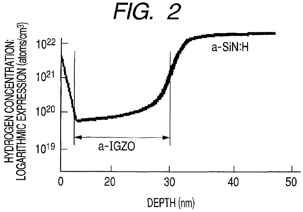
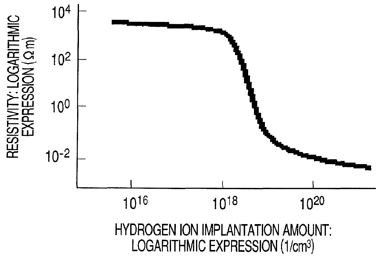
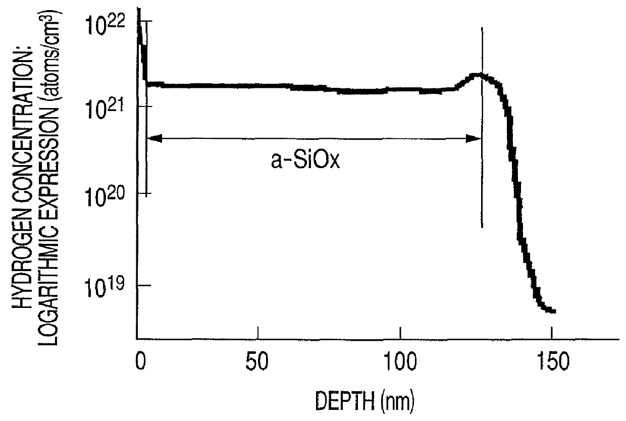
[0011]The present invention has been accomplished to dissolve the above described problems, and provides a display apparatus which can be stably driven for a long period of time without degrading the high mobility and high characteristics peculiar to an oxide semiconductor, and can display an image with high definition and less image defect, and a production method of the display apparatus.
[0014]According to the present invention, a display apparatus is provided which can display an image with high definition and less image defect, because a transistor with an active layer which includes an oxide containing In and Zn and at least a part of which is amorphous can stably perform driving for a long period of time. Thereby, the present invention can provide a bottom-emission type display apparatus, a top-emission type display apparatus or a two-sided emission type high-luminance display apparatus which maintains superior stability for a long period of time.

Problems solved by technology

However, since In2O3 of a main raw material of ITO contains a rare metal, and it has been feared whether a desired amount of ITO can also be steadily supplied in future.
Accordingly, there has been a problem that degradation of the characteristics may sometimes be caused due to the phenomenon.
Moreover, the degradation of the characteristics has been intensively occurred during active matrix driving for a long period of time.
As described above, the conventional oxide semiconductor has the problem that when used in a stacked device, if a large amount of hydrogen is contained in an insulating layer, the degradation of the characteristics is liable to be occurred due to diffusion of the hydrogen.
The problem has remarkably appeared in a display apparatus which employs the oxide semiconductor particularly for an active layer of a TFT.
In this case, there has been a problem that a display apparatus cannot be realized which is stably driven for a long period of time and displays an image with high definition and less image defect.

Method used


Image

  • Display apparatus using oxide semiconductor and production method thereof
  • Display apparatus using oxide semiconductor and production method thereof
  • Display apparatus using oxide semiconductor and production method thereof

Examples


application example

[0095]A configuration example in which the above described embodiment is applied to a display apparatus having a plurality of matrix wirings will now be described with reference to FIG. 8.

[0096]In the figure, reference numeral 55 denotes a selecting transistor which selects a pixel, and reference numeral 56 denotes a driving transistor which drives a light-emitting layer 58. In addition, a capacitor 57 is provided for keeping a selected state, stores an electric charge between a GND line 53 and a source electrode of the selecting transistor 55, and holds a signal of a gate of the driving transistor 56. The pixel is selected by a scanning electrode line 51 and a signal electrode line 52.

[0097]Specifically, the operation will now be described. An image signal from a driver circuit (not shown) is applied to a gate electrode in a form of a pulse signal through the scanning electrode line 51. At the same time, another pulse signal from another driver circuit (not shown) is applied to the...

example 1

[0106]In the first place, Example 1 according to the present invention will now be described.

[0107]At first, a SiO2 glass substrate (1737 manufactured by Corning, Inc.) was prepared as a substrate for film formation. As the pretreatment before film formation, the substrate was ultrasonically degreased and cleaned with acetone, IPA (isopropanol), and ultrapure water sequentially for five minutes each and then dried at 100° C. in air.

[0108]Subsequently, a film with a thickness of 200 nm was deposited by a DC (direct current) sputtering process using Al—Si (5%) as a target material, and then a power supply line, a GND line, and a signal electrode line were patterned at desired positions by using a photolithographic process and a dry process.

[0109]Next, a film of a-SiNx:H was deposited thereon as an interlayer insulating layer in a thickness of 600 nm at a substrate temperature of 300° C. using a plasma-CVD process. Subsequently, contact holes were formed in desired positions, and elect...

example 2

[0120]In the next place, Example 2 according to the present invention will be described.

[0121]At first, as a substrate, a SiO2 glass substrate (1737 manufacture by Corning Inc.) was prepared which had an ITO film with a resistivity of 1.4×10⁻⁴ Ω·cm and a thickness of 100 nm formed thereon. As the pretreatment before film formation, the substrate was ultrasonically degreased and cleaned with acetone, IPA, and ultrapure water sequentially for five minutes each and then dried at 100° C. in air.

[0122]Subsequently, a lower electrode of a light-emitting layer was patterned by a photolithographic process and a wet process.

[0123]Subsequently, a film with a thickness of 200 nm was deposited by a DC sputtering process using Al—Si (5%) as a target material, and then a power supply line, a GND line, and a signal electrode line were patterned at desired positions by using a photolithographic process and a dry process. At this time, patterning was performed such that the lower electrode and the p...


PUM


Abstract

A display apparatus includes a light-emitting layer, a pair of electrodes sandwiching the light-emitting layer, a transistor with an active layer for driving the light-emitting layer through the pair of the electrodes, and a matrix wiring portion having a scanning electrode line, a signal electrode line, and a first insulating layer. The active layer has an oxide which contains In and Zn and at least a part of which is amorphous, and further includes a second insulating layer containing hydrogen in an amount of less than 3×10²¹ atoms / cm3 disposed between the active layer and the first insulating layer.

Description

TECHNICAL FIELD[0001]The present invention relates to a display apparatus using an oxide semiconductor and a production method thereof, and in particular, relates to a top-emission type, bottom-emission type or two-sided emitting type organic electroluminescent display apparatus or inorganic electroluminescent display apparatus.BACKGROUND ART[0002]ITO (Indium Tin oxide) has been used for a transparent electrode in a transmission type liquid crystal device. However, since In2O3 of a main raw material of ITO contains a rare metal, and it has been feared whether a desired amount of ITO can also be steadily supplied in future. Japanese Patent Application Laid-Open No. 2000-044236 proposes a method of producing a new transparent conductor material which has a reduced content of In2O3, has a low electrical resistance, has an optical absorption edge in ultraviolet region and has an excellent blue light transmissivity; and an electrode material using the material.[0003]In addition, material...

Claims


Application Information

Patent Timeline
Patent Type & Authority Patents(United States)
IPC IPC(8): H01L51/50H01L51/52H01L51/56H01L51/54
CPCH01L29/7869H01L27/3244H10K59/12H01L27/1225H01L27/1248H01L29/78693H10K59/1213
Inventor SANO, MASAFUMITAKAHASHI, KENJI
Owner CANON KK
Why Eureka
Try Eureka