Oxide etching method

a technology of oxide film and etching method, which is applied in the manufacture of final products, basic electric elements, chemistry apparatus and processes, etc., can solve the problems of reducing the production yield, contaminating the photoresist into a formed film, and melted photoresist at a high temperature, so as to achieve remarkable selectivity, precise and highly selective wet etching, and the effect of not variable performan

Inactive Publication Date: 2012-05-01
CANON KK
View PDF30 Cites 122 Cited by
  • Summary
  • Abstract
  • Description
  • Claims
  • Application Information

AI Technical Summary

Benefits of technology

[0015]The present invention also provides an etching method by which precise and easy etching can be performed in a thin film semiconductor device containing two or more kinds of oxide films selected from IGZO, IZO, IGO, and ITO.
[0021]According to the present invention described above, precise and highly selective wet etching can be performed in a thin film semiconductor device including two or more kinds of oxide films selected from IGZO, IZO, IGO, and ITO. Further, the thin film semiconductor device produced by the etching method of the present invention and by using the etching liquid having remarkable selectivity of the present invention is advantageous in that the device performance is not variable and is stabile and uniform, and that the device productions steps are simple and easy to carry out.

Problems solved by technology

However, the lift-off process as described above has a problem that a photoresist is melted and deformed at a high temperature.
The lift-off process has another problem that when a photoresist is removed, an edge of a pattern of a deposited film is curved up, and thereafter an electric wire crossing over the pattern edge is liable to be broken, which lowers the production yield.
In particular, there is a pollution problem that a photoresist is contaminated into a formed film due to a lift-off step.
However, maintenance costs for a dry etching apparatus body, a circumferential gas supply system, exhaust gas processing of a chlorine-based gas, power consumption and the like are remarkably large, and there is also a problem of short life of the apparatus due to particle contamination or the like.
Further, there is a case where the control of highly selective etching is difficult due to ion impact.
In addition, when considering future production of large area displays, there is a fear that high capacities and large costs are necessary for a chamber, a vacuum system, and the like of the dry etching apparatus.
In contrast, in the wet etching, the etching proceeds isotropically, so that there arises a problem of generating a phenomenon such as an undercut beneath a mask.
If the etch selectivity is insufficient, there are cases where a material not to be etched may be etched, which may increase variation in the performance of electronic devices, thus resulting in reduction of the yield.

Method used


Image

  • Oxide etching method
  • Oxide etching method
  • Oxide etching method

Examples


example 1

Etch Rate Measurement

[0058]In Example 1, a specific example of an etching method of an indium oxide film including IZO, IGZO, IGO, and ITO of the present invention will be described.

[0059]First, experimental samples are produced according to a procedure described below. A Si substrate (525 mm in thickness) having a 100 nm thick Si thermal oxide film provided thereon is used as a base. Three oxide films of an IGZO film, an IZO film, and an IGO film are formed on the Si substrate with the Si thermally oxide film by reactive sputtering under the conditions shown in Table 1 below.

[0060]Incidentally, indium oxide thin films of IGZO, IZO, and IGO each containing microcrystals are deposited on the substrate by the above-mentioned spattering film deposition method. Considering that the incidence X-ray diffraction (angle of incidence: 0.5°) of the IGZO, IZO, and IGO thin films shows no clear diffraction peak, it can be said that the produced IGZO, IZO, and IGO thin films are amorphous.

[0061]...

example 2

Stack Structure

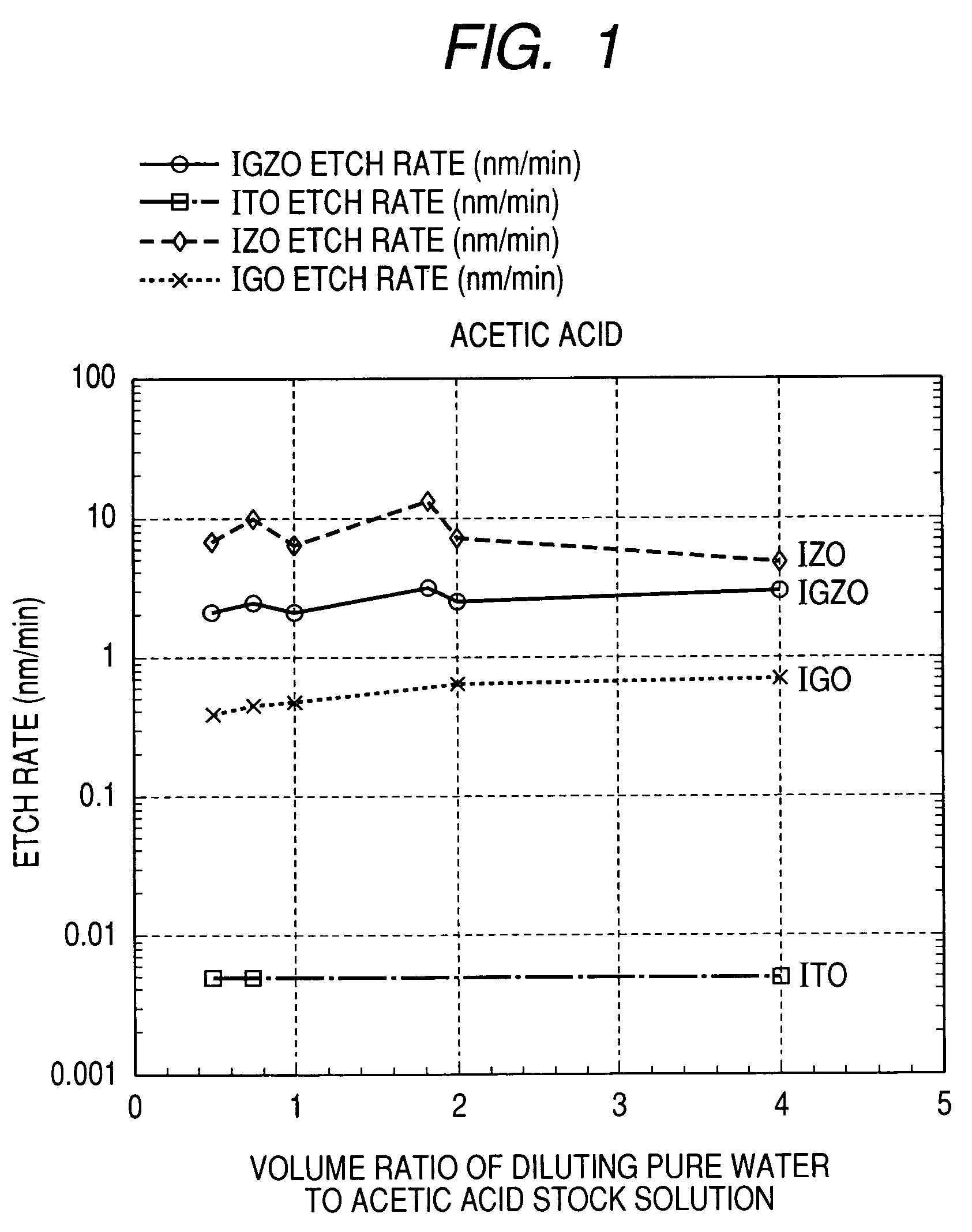
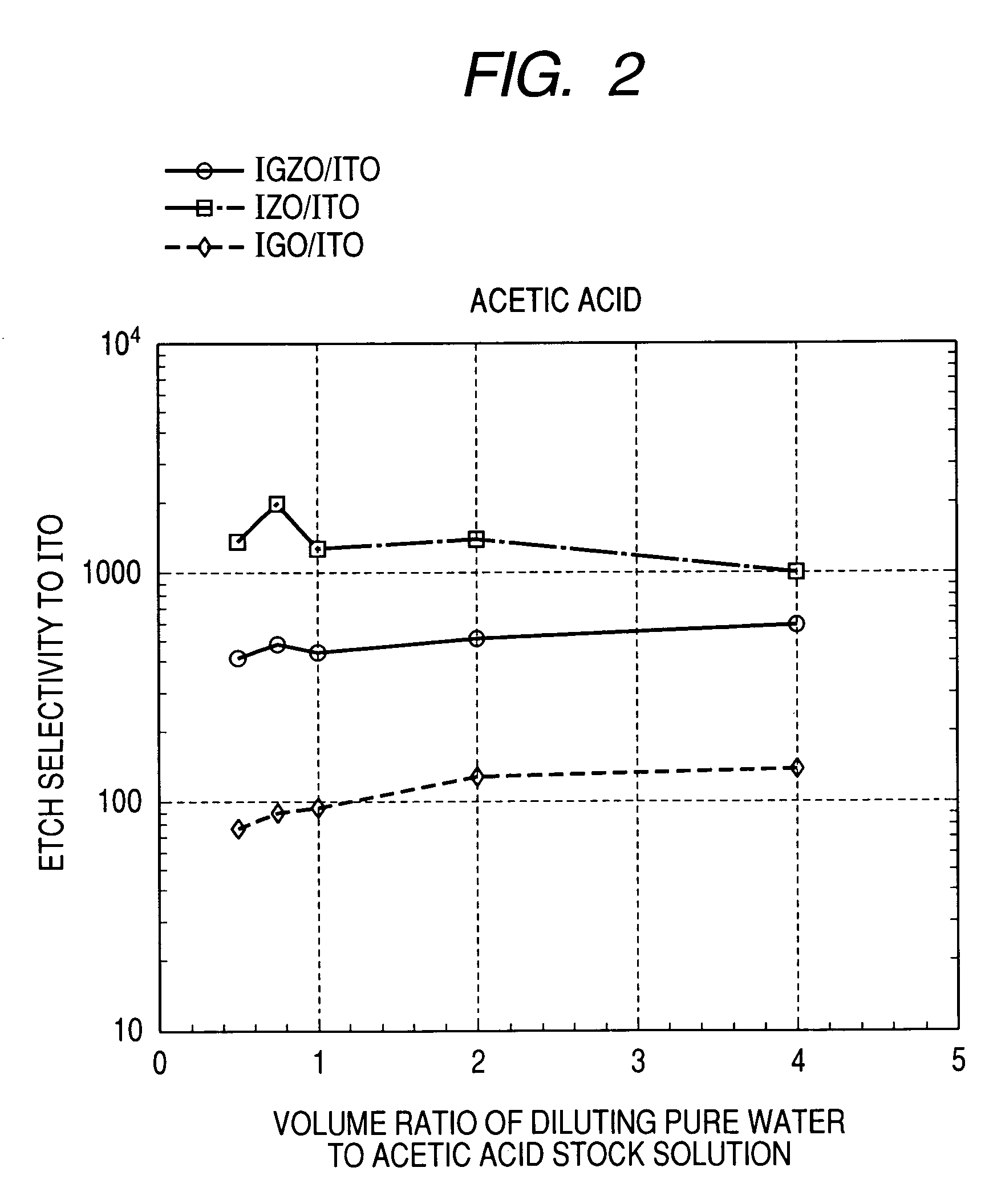
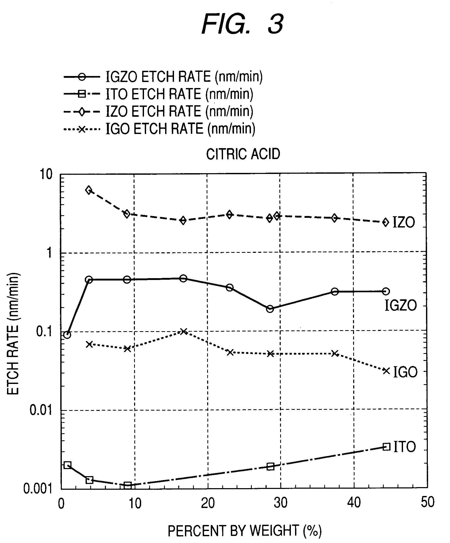
[0095]FIGS. 11A and 11B are cross-sectional views illustrating the most common etching form according to an example of the present invention. A layer 1 is a material layer with a lower etch rate, a layer 2 is a material layer with a higher etch rate, and a layer 3 (resist layer) is used as an etching mask. In usual, when the selectivity of the layers 1 and 2 of FIGS. 11A and 11B is low, the depth of excessively etched area Δd of the layer 1 of FIG. 11B and an undercut amount Δw of the layer 2 are close to each other, resulting in variation of thin film transistor devices due to etching. It can be seen that with the use of the etching liquids of Example 1, the etch rates of oxides containing indium have the relationship of IZO>IGZO>IGO> and ITO. According to the present invention, when the layer 1 of FIGS. 11A and 11B is an ITO layer and the layer 2 is one material selected from the group consisting of IZO, IGZO, and IGO, there can be obtained the highly selective etch...

example 3

Top-Gate Bottom-Contact TFT

[0096]FIG. 12 is a schematic cross-sectional view illustrating a structure of a top-gate bottom-contact thin film transistor according to one example of the present invention. Reference numerals 4, 5, 6, 7, 8, and 9 denote a substrate (e.g., glass substrate), drain electrode, source electrode, active layer (channel layer), gate insulation film, and gate electrode, respectively. Reference character L denotes a channel length. FIGS. 14A to 14K are schematic cross-sectional views illustrating production steps of a top-gate bottom-contact thin film transistor as shown in FIG. 12 using the etching liquid of Example 1 of the present invention. As shown in FIG. 14A, a glass plate having a thickness of 500 mm (manufactured by Corning; trade name: Corning 1737 glass; glass transition temperature: 640° C.) is used as the substrate 4. A polycrystalline ITO film with a thickness of 250 nm is formed on the surface of the substrate 4 by reactive sputtering, and the drai...


PUM

PropertyMeasurementUnit
temperatureaaaaaaaaaa

Abstract

There is provided an etching method of an amorphous oxide layer containing In and at least one of Ga and Zn, which includes etching the amorphous oxide layer using an etchant containing any one of acetic acid, citric acid, hydrochloric acid, and perchloric acid.

Description

[0001]This application claims the benefit of Japanese Patent Application No. 2006-209859, filed Aug. 1, 2006, which is incorporated herein by reference in its entirety.TECHNICAL FIELD[0002]The present invention relates to an etching method of an oxide film containing In, Ga, and Zn with a high selectivity with respect to ITO (Indium Tin Oxide). More specifically, the present invention relates to a highly selective etching method of an oxide containing In and Zn and an oxide containing In and Ga which is employed in producing a fine electronic component such as a semiconductor device, a semiconductor integrated circuit, and an electrode.BACKGROUND ART[0003]In recent years, under circumstances where reductions in size, weight, and power consumption of electronic equipments have been advanced, transparent oxide semiconductors and transparent conductive oxides have been drawing attention in a field of display. In particular, since a film can be formed on a resin film at low temperatures...

Claims


Application Information

Patent Timeline
Patent Type & Authority Patents(United States)
IPC IPC(8): H01L21/302
CPCC09K13/04C09K13/06H01L29/78693H01L31/022466H01L31/1804Y02E10/547H01L31/022475H01L31/022483Y02P70/50H01L21/306H01L31/18H01L31/0224
Inventor CHANG, CHIENLIU
Owner CANON KK
Why Eureka
Try Eureka