Thin film field effect transistor and display

a field effect transistor and thin film technology, applied in the direction of solid-state devices, electric lighting sources, electric light sources, etc., can solve the problems of poor heat resistance, low heat resistance, and difficulty in forming transistors directly on resin substrates

Active Publication Date: 2012-05-29
SAMSUNG DISPLAY CO LTD
View PDF12 Cites 543 Cited by
  • Summary
  • Abstract
  • Description
  • Claims
  • Application Information

AI Technical Summary

Benefits of technology

[0049]When ΔE is less than 0.1 eV, since the difference between the band gap of the active layer and the band gap of the resistance layer is excessively small, there is not difference in view of the operation as a device and the effect of the invention cannot be obtained. Further, when ΔE is 13.0 eV or more, since the difference between the band gap of the active layer and the band gap of the resistance layer is excessively large, barriers for electrons to movement from the source electrode to the active layer or from the active layer to the drain electrode are often increased excessively, and ON current decreases, which is not preferable.
[0050]Preferably, a carrier concentration of the active layer is higher than a carrier concentration of the resistance layer.
[0051]Preferably, the amorphous oxide semiconductor in the active layer includes at least one element selected from the group consisting of In, Sn, Zn, and Cd.
[0052]Preferably, the amorphous oxide in the resistance layer includes at least one element selected from the group consisting of Ga, Mg, Al, Ca, and Si.
[0053]Preferably, the active layer and the resistance layer are layers each formed by a sputtering method.
[0055]The TFT of the invention is to be described in the following in more detail.

Problems solved by technology

However, fabrication of the transistors using the silicon thin films described above requires a thermal treatment process at a relatively high temperature, and it is difficult to form the transistors directly on a resin substrate which is generally low in heat resistance.
Accordingly, such an active layer is difficult to form directly on a resin substrate that is poor in heat resistance.
However, while the TFT can be utilized as a liquid crystal screen control TFT using a glass substrate, it is difficult to fabricate the TFT on a flexible resin substrate since the flexible resin substrate intrinsically involves the problem of heat resistance described above.
However, when an amorphous oxide semiconductor is used in an active layer of a TFT, an OFF current is high, and accordingly, there is a problem in that an ON / OFF ratio is low.
That is, there still remain many problems to be overcome.

Method used


Image

  • Thin film field effect transistor and display
  • Thin film field effect transistor and display
  • Thin film field effect transistor and display

Examples


example 1

1. Preparation of TFT Element

1) Preparation of Inventive TFT Element
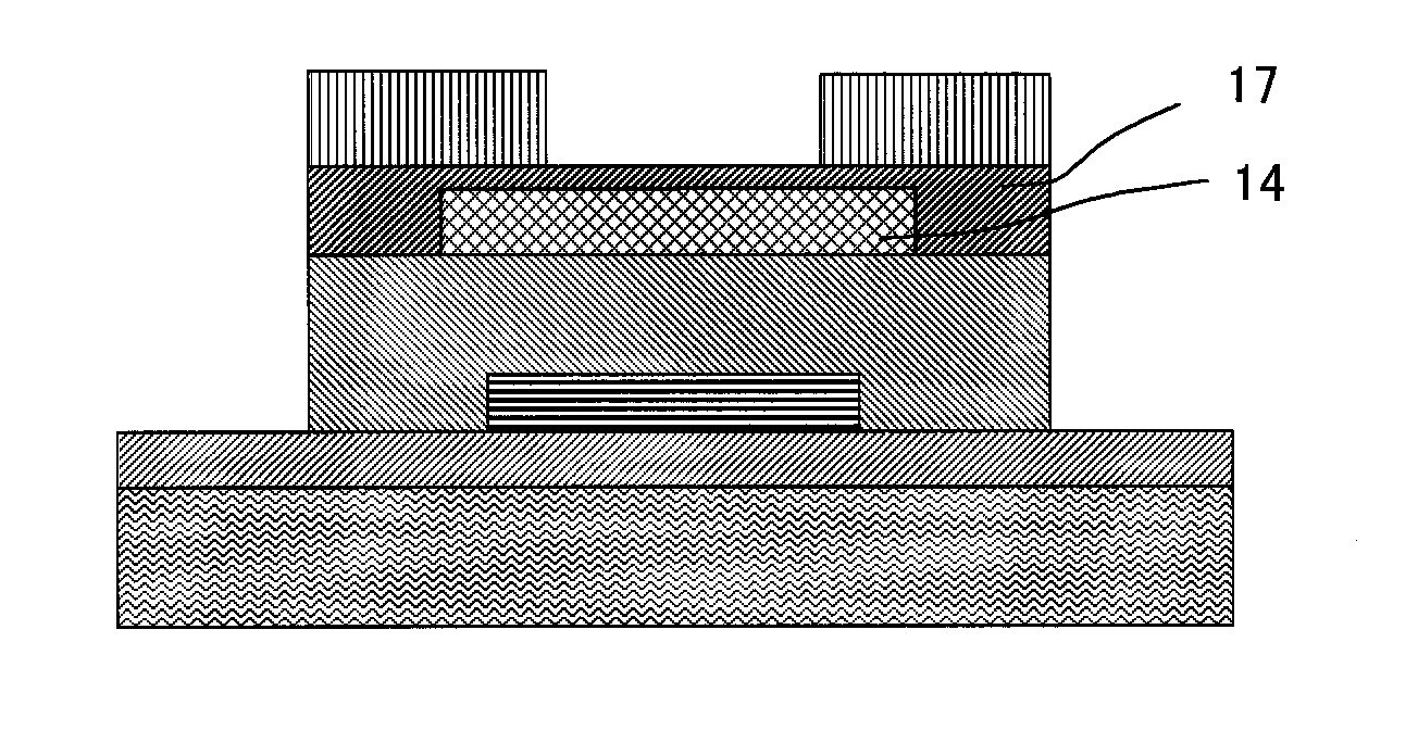
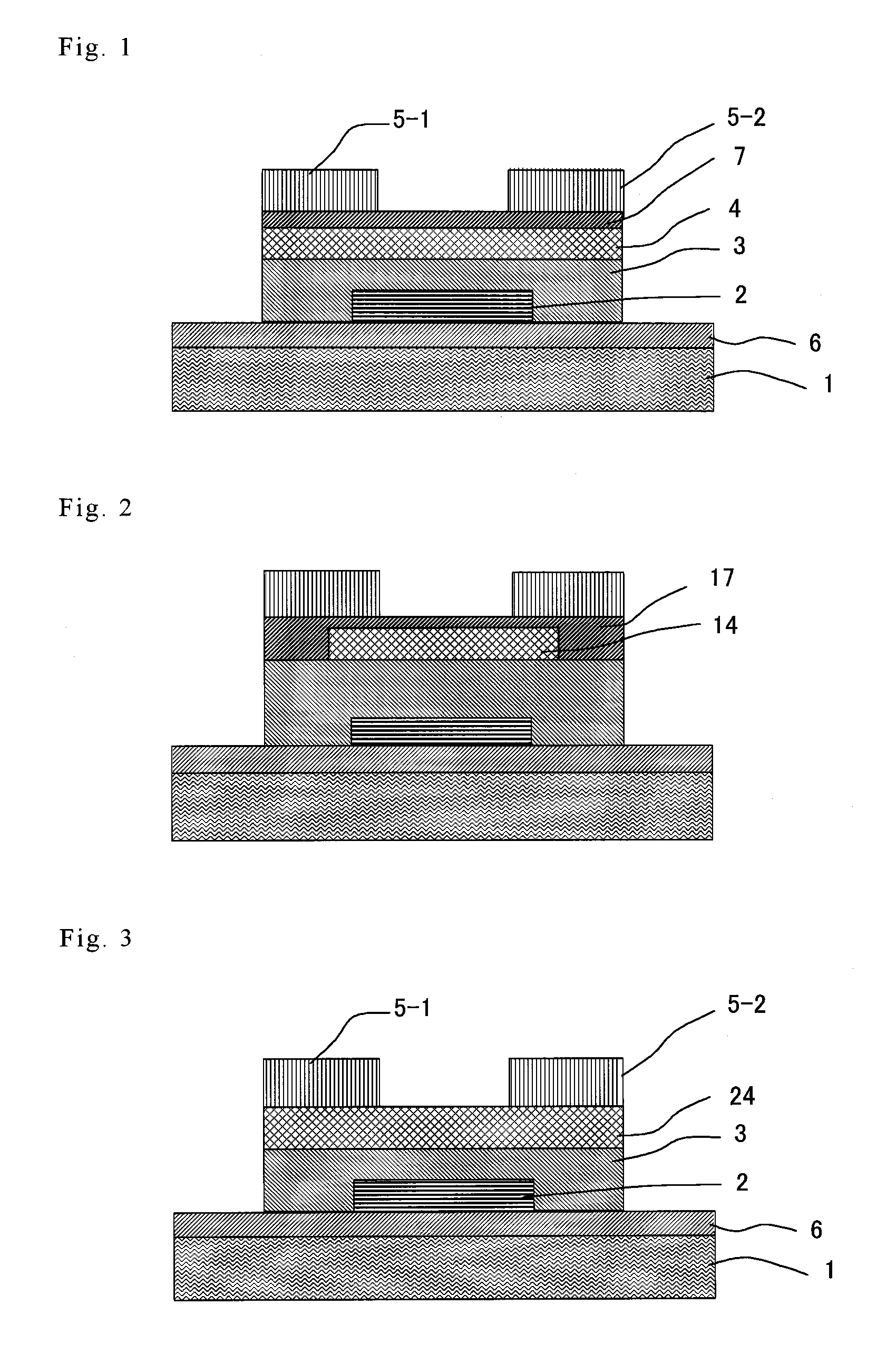
[0295]

[0296]A substrate and a gate electrode were prepared as follows.

[0297]An N-type Si substrate having a thickness of 0.5 mm (manufactured by Jemco Co., Ltd., electric resistance: from 1 Ωcm to 3.5 Ωcm) was used as a conductive N-type substrate, and this is used as both the substrate and the gate electrode.

[0298]

[0299]Next, on the gate electrode, the following gate insulating layer was formed.

[0300]Gate insulating layer: a gate insulating layer was provided by performing RF magnetron sputtering vacuum deposition of SiO2 (conditions: target of SiO2, temperature for film formation of 54° C., flow rates of sputtering gas Ar / O2=12 sccm / 2 sccm, RF power of 400 W, and film-forming pressure of 0.4 Pa) to form a layer having a thickness of 100 nm. Patterning of the SiO2 gate insulating layer was performed using a shadow mask during sputtering.

[0301]

[0302]Active layer 1: on the gate insulating layer, RF magnetron sputteri...

example 2

[0329]TFT elements were prepared in a similar manner to that in Example 1, except that a barrier-attached film having the following insulating layer, which has a function of barrier, on both sides of a polyethylene naphthalate film (having a thickness of 100 μm) was used instead of the n-Si substrate in Example 1.

[0330]Insulating layer: SiON was deposited to give a thickness of 500 nm. For the deposition of SiON, an RF magnetron sputtering deposition method (conditions for sputtering: target of Si3N4, RF power of 400 W, flow rates of gas Ar / O2=12 sccm / 3 sccm, and film-forming pressure of 0.45 Pa) was applied.

[0331]The obtained elements were evaluated in a similar manner to that in Example 1. As a result, the inventive elements exhibited a small shift quantity of threshold voltage, similar to the results in Example 1.

example 3

1. Preparation of Organic EL Display

[0332](Preparation of Organic EL Element Part)

[0333]1) Formation of Lower Electrode

[0334]As a substrate, the above barrier-attached film including an insulating layer having a function of barrier on both sides of a polyethylene naphthalate film was used. On the substrate, indium-tin oxide (which is referred to hereinafter as ITO) was deposited at a thickness of 150 nm to form an anode.

[0335]2) Formation of Organic Layer

[0336]After cleaning, a hole injection layer, a hole transport layer, a light-emitting layer, a hole blocking layer, an electron transport layer and an electron injection layer were disposed in this order.

[0337]The composition of each layer is as follows. Each layer was provided by resistance heating vacuum deposition.

[0338]Hole injection layer: a layer containing 4,4′,4″-tris(2-naphthylphenylamino)triphenylamine (which is referred to as 2-TNATA) and 2,3,5,6-tetrafluoro-7,7,8,8-tetracyanoquinodimethane (which is referred to as F4-TC...


PUM


Abstract

A TFT is provided which includes, on a substrate, at least a gate electrode, a gate insulating layer, an active layer containing an amorphous oxide semiconductor, a source electrode and a drain electrode, wherein a resistance layer containing an amorphous oxide and having a thickness of more than 3 nm is disposed between the active layer and at least one of the source electrode or the drain electrode, and a band gap of the active layer is smaller than a band gap of the resistance layer. Also, a display using the TFT is provided.

Description

CROSS-REFERENCE TO RELATED APPLICATION[0001]This application claims priority under 35 USC 119 from Japanese Patent Application No. 2008-76493, the disclosure of which is incorporated by reference herein.BACKGROUND OF THE INVENTION[0002]1. Field of the Invention[0003]The present invention relates to a thin film field effect transistor and a display using the same. Particularly, it relates to a thin film field effect transistor in which an amorphous oxide semiconductor is used for an active layer, and a display using the same.[0004]2. Description of the Related Art[0005]In recent years, flat panel displays (FPDs) have been put to practical use, due to the progress made in liquid crystal and electroluminescence (EL) technologies, etc. Especially, an organic electroluminescence element (hereinafter referred to as an “organic EL element” in some cases) formed using a thin film material which emits light by excitation due to application of electric current can provide light emission of hi...

Claims


Application Information

Patent Timeline
Patent Type & Authority Patents(United States)
IPC IPC(8): H01L29/04H05B44/00
CPCH01L29/78618H01L29/7869H01L29/78696H01L29/45
Inventor ITAI, YUICHIRO
Owner SAMSUNG DISPLAY CO LTD
Why Eureka
Try Eureka