Growth of germanium epitaxial thin film with negative photoconductance characteristics and photodiode using the same

a thin film, negative technology, applied in the direction of crystal growth process, polycrystalline material growth, manufacturing tools, etc., can solve the problems of reducing the efficiency of the device manufacturing process, affecting so as to reduce the pressure of chemical vapor deposition and improve the quality of the device. , the effect of excellent mass production

Active Publication Date: 2012-05-29
ELECTRONICS & TELECOMM RES INST
View PDF9 Cites 22 Cited by
  • Summary
  • Abstract
  • Description
  • Claims
  • Application Information

AI Technical Summary

Benefits of technology

[0014]The present invention is directed to a method of growing a high-quality germanium (Ge) epitaxial thin film in which penetrating dislocation density is adjusted by a three-stage growth method including low, rising and high temperatures using reduced pressure chemical vapor deposition (RPCVD) that exhibits excellent mass production, and surface roughness is reduced.
[0015]The present invention is also directed to a photodiode including a high-quality germanium (Ge) epitaxial thin film in which penetrating dislocation density is adjusted, and surface roughness is reduced.

Problems solved by technology

A rough surface with a wave pattern may be an obstacle to a process of fabricating a device.
The penetrating dislocation which is propagated to the surface may serve as a defect in a thin film to be formed thereon, and device characteristics may be deteriorated or a leakage current may be generated.
However, the existing adjusted diffraction factors may function to enable carriers to cause transition effects between energy valleys, and thus negative resistance effects may occur.
This process is performed using costly ultra-high vacuum chemical vapor deposition (UHVCVD) equipment that is unsuitable for commercialization, and takes four hours to complete only a post-annealing process.

Method used


Image

  • Growth of germanium epitaxial thin film with negative photoconductance characteristics and photodiode using the same
  • Growth of germanium epitaxial thin film with negative photoconductance characteristics and photodiode using the same
  • Growth of germanium epitaxial thin film with negative photoconductance characteristics and photodiode using the same

Examples


example 1

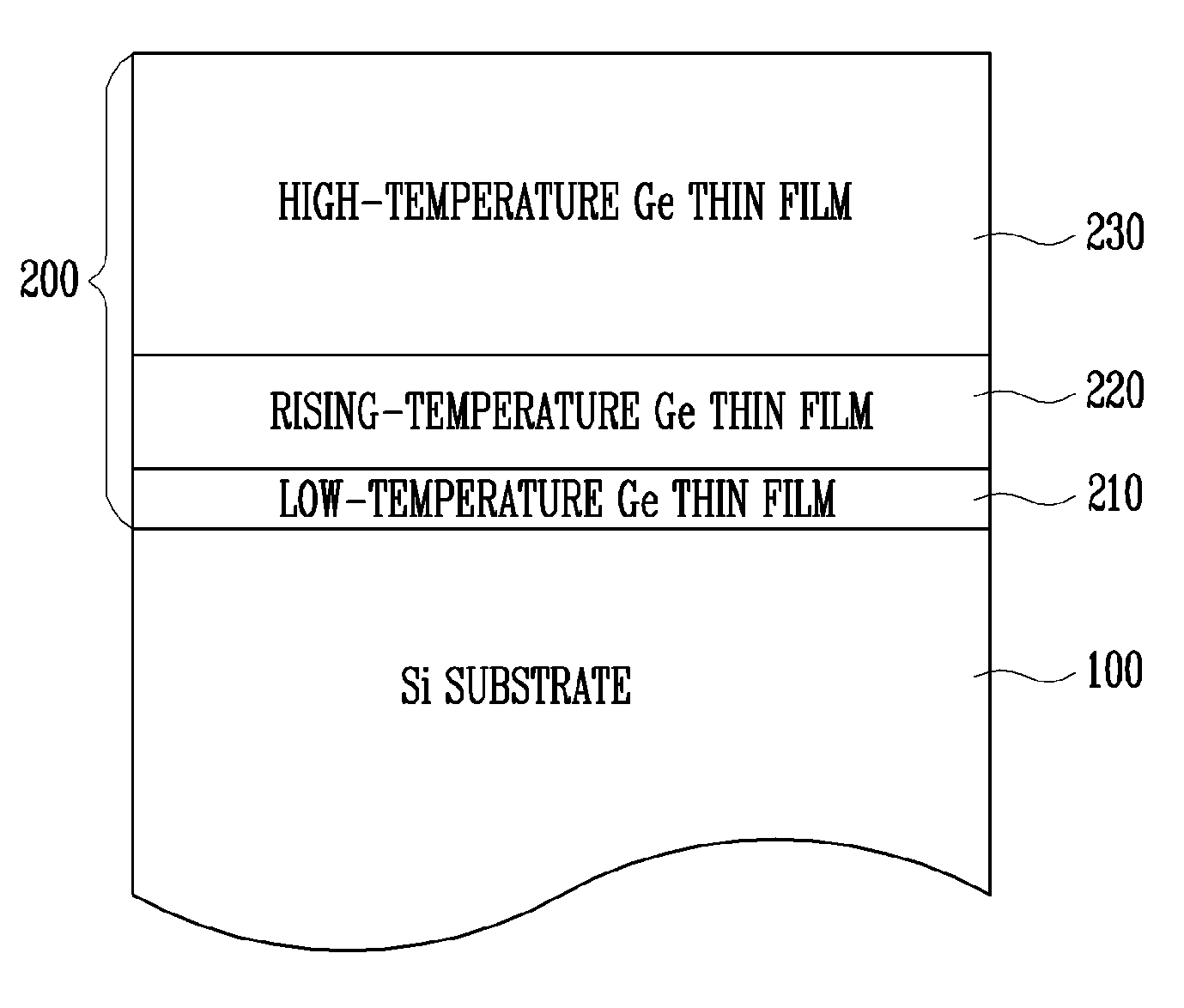
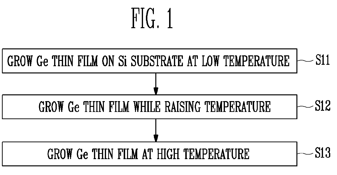
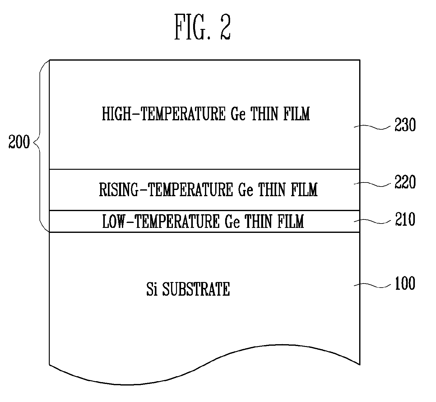
[0047]Growing Low-Temperature Germanium (Ge) Thin Film

[0048]Under RPCVD conditions, a low-temperature germanium (Ge) thin film 210 was deposited to be grown on a silicon substrate 100 to a thickness of 100 nm at a deposition rate of 100 Å / min by flowing GeH4 gas diluted into 20 vol % with hydrogen at a flow rate of 150 sccm under a temperature of 420° C. and a pressure of 60 Torr, and flowing hydrogen gas as a carrier gas at a flow rate of 20 slm.

[0049]Growth of Rising-Temperature Germanium (Ge) Thin Film

[0050]Then, under RPCVD conditions, a temperature of the low temperature germanium (Ge) thin film 210 was raised from 420° C. to 680° C. at a rate of 12° C. per minute, and GeH4 gas was injected at a flow rate of 10 sccm under a pressure of 60 Torr, and thus a rising-temperature germanium (Ge) thin film 220 was grown to a thickness of 200 nm at the same deposition rate as that of the low-temperature germanium (Ge) thin film.

[0051]Growth of High-Temperature Germanium (Ge) Thin Film

[0...

experimental example

[0053]Observation through Transmission Electron Microscope (TEM)

[0054]A cross section of the low-temperature germanium (Ge) thin film 210 grown in Example 1 was observed through a TEM, and the observed results are illustrated in FIG. 3. Further, a TEM with high resolution was used to confirm crystallinity, and the confirmed results are illustrated in FIG. 4.

[0055]Further, a cross section of a germanium (Ge) epitaxial thin film 200 grown by a three-stage growth method including low, rising and high temperatures in Example 1 was confirmed by a TEM, and the confirmed results are illustrated in FIG. 5.

[0056]It can be observed through FIG. 3 that misfit dislocations were generated across the entire surface of the low-temperature germanium (Ge) thin film 210 to alleviate a stress caused by a difference in lattice constant between silicon (Si) and germanium (Ge), most of the dislocations spread onto the surface in the shape of penetrating dislocations, and reduced surface roughness was exh...


PUM

PropertyMeasurementUnit
thicknessaaaaaaaaaa
thicknessaaaaaaaaaa
temperatureaaaaaaaaaa

Abstract

A method of growing a germanium (Ge) epitaxial thin film having negative photoconductance characteristics and a photodiode using the same are provided. The method of growing the germanium (Ge) epitaxial thin film includes growing a germanium (Ge) thin film on a silicon substrate at a low temperature, raising the temperature to grow the germanium (Ge) thin film, and growing the germanium (Ge) thin film at a high temperature, wherein each stage of growth is performed using reduced pressure chemical vapor deposition (RPCVD). The three-stage growth method enables formation of a germanium (Ge) epitaxial thin film characterized by alleviated stress on a substrate, a lowered penetrating dislocation density, and reduced surface roughness.

Description

CROSS-REFERENCE TO RELATED APPLICATION[0001]This application claims priority to and the benefit of Korean Patent Application Nos. 10-2008-0121611, filed Dec. 3, 2008 and 10-2009-0025685, filed Mar. 26, 2009, the disclosure of which is incorporated herein by reference in its entirety.BACKGROUND[0002]1. Field of the Invention[0003]The present invention relates to a method of growing a germanium (Ge) epitaxial thin film required for fabricating a germanium (Ge) photodiode, and more particularly, to a method of growing a germanium (Ge) epitaxial thin film having superior characteristics of relaxed stress, low penetrating dislocation density, and reduced surface roughness on a silicon substrate using reduced pressure chemical vapor deposition (RPCVD), and a photodiode using the same.[0004]2. Discussion of Related Art[0005]A new device using a silicon (Si) and silicon-germanium (SiGe) or germanium (Ge) heterojunction structure has been developed in the last several decades.[0006]In partic...

Claims


Application Information

Patent Timeline
Patent Type & Authority Patents(United States)
IPC IPC(8): H01L31/028C03B23/06
CPCC30B25/10C30B25/16C30B29/08H01L21/02381H01L21/0245H01L21/02502H01L21/02532H01L21/0262H01L31/028H01L31/103H01L31/1808Y02E10/547
Inventor KIM, SANG HOONKIM, GYUNG OCKSUH, DONG WOOJOO, JI HO
Owner ELECTRONICS & TELECOMM RES INST
Why Eureka
Try Eureka