
Semiconductor device and manufacturing method thereof

a technology of semiconductor layer and manufacturing method, which is applied in the direction of semiconductor device, semiconductor/solid-state device details, electrical apparatus, etc., can solve the problems of inoperable tft, increased power consumption of tft, etc., and achieve the effect of preventing the thinning or removal of a semiconductor layer, lowering contact resistance, and reducing power consumption

Active Publication Date: 2012-08-28
SEMICON ENERGY LAB CO LTD
View PDF46 Cites 11 Cited by
  • Summary
  • Abstract
  • Description
  • Claims
  • Application Information

AI Technical Summary

Benefits of technology

The present invention provides an element structure of a semiconductor device that can obtain a sufficient contact area between an electrode in contact with a source or drain region and the source or drain region, while preventing overetching. The invention also provides a method for manufacturing this semiconductor device. The semiconductor device includes an upper electrode that is larger than the contact hole, and a lower electrode that is in contact with the upper electrode. The invention also provides a semiconductor device with a sandwich structure between the upper and lower electrodes, and a silicide layer formed between the electrodes and the impurity region. The invention also provides a semiconductor device with a contact hole that overlaps with a region where the electrodes are stacked, and a wiring in contact with the upper electrode. The invention aims to improve the performance and reliability of semiconductor devices.

Problems solved by technology

Higher contact resistance increases power consumption of a TFT.
Too high contact resistance can result in inoperativeness of the TFT.

Method used


Image

  • Semiconductor device and manufacturing method thereof
  • Semiconductor device and manufacturing method thereof
  • Semiconductor device and manufacturing method thereof

Examples


embodiment mode 1

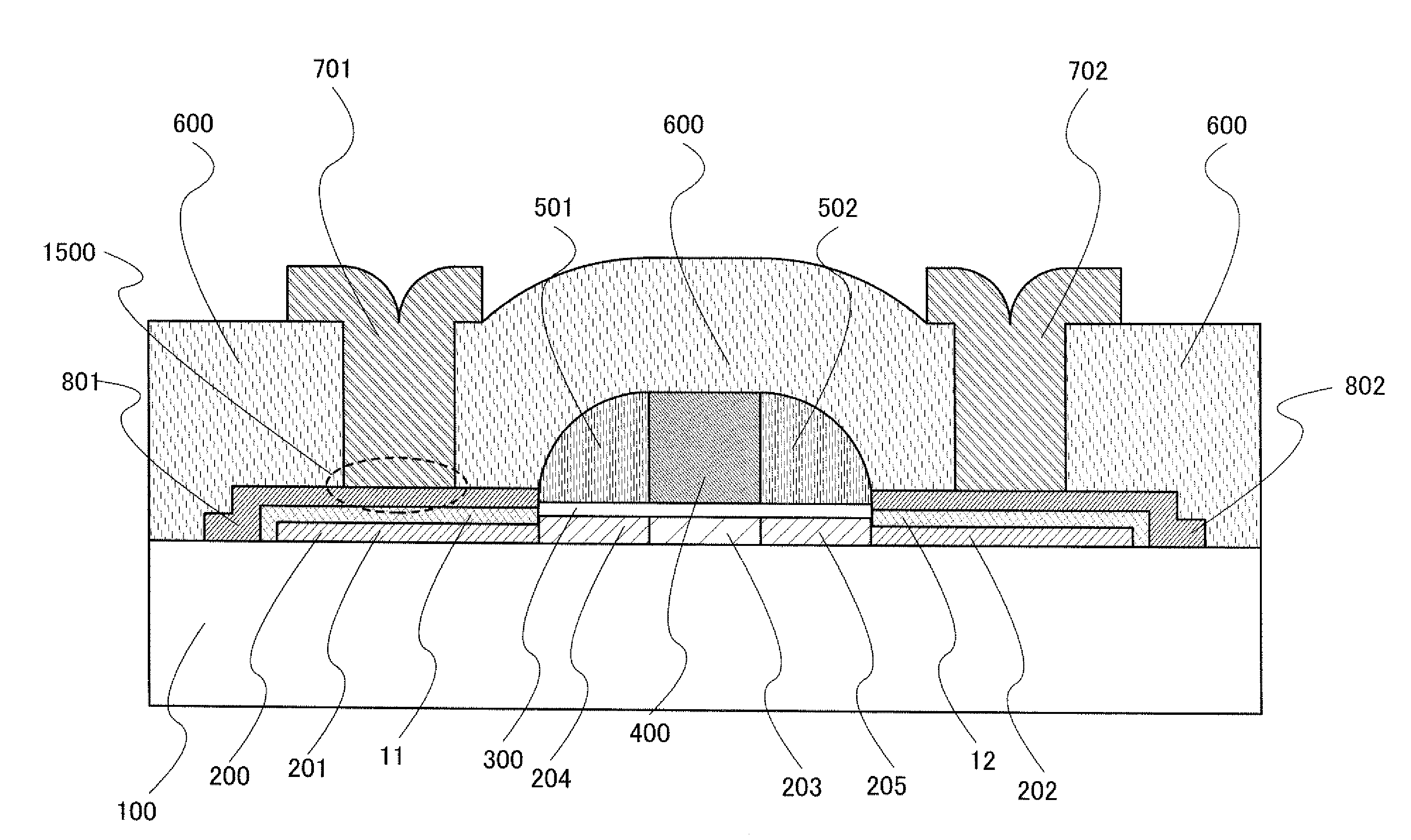
[0067]A semiconductor device of this embodiment mode is described with reference to FIG. 1.

[0068]The semiconductor device of this embodiment mode includes an insulator 100, a semiconductor layer 200 (of an island shape), a gate insulating film 300, a gate electrode 400, a sidewall 501, a sidewall 502, an interlayer insulating film 600, a wiring 701, a wiring 702, an upper electrode 801, and an upper electrode 802 (see FIG. 1).

[0069]The insulator 100 is a base insulating film formed over a substrate, or a substrate.

[0070]The semiconductor layer 200 is formed over the insulator 100.

[0071]The semiconductor layer 200 includes a channel formation region 203 placed between a source region 201 and a drain region 202.

[0072]The source region 201 and the drain region 202 are high-concentration impurity regions that are formed by adding an impurity element imparting conductivity to parts of the semiconductor layer 200 at a high concentration. In this embodiment mode, phosphorus, which is an el...

embodiment mode 2

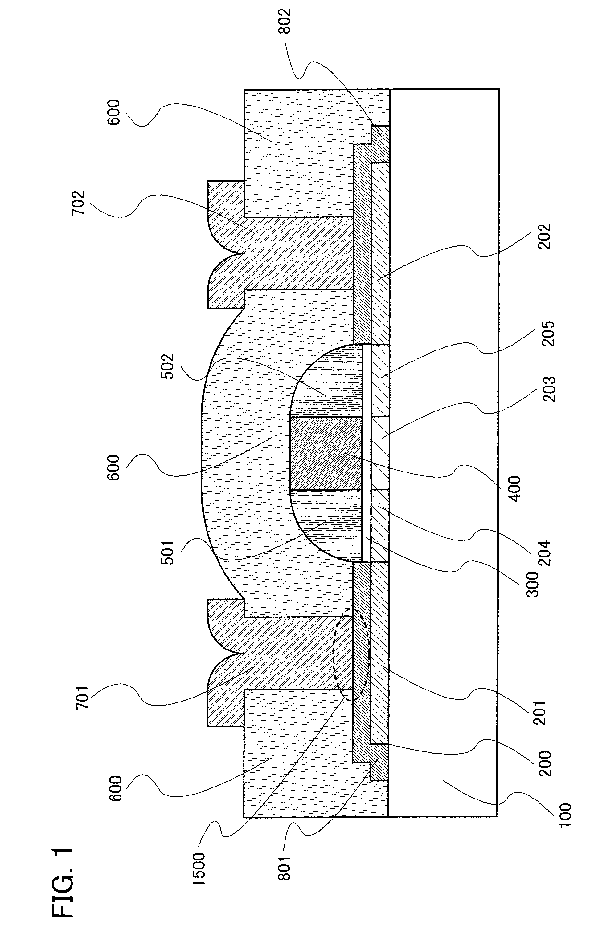
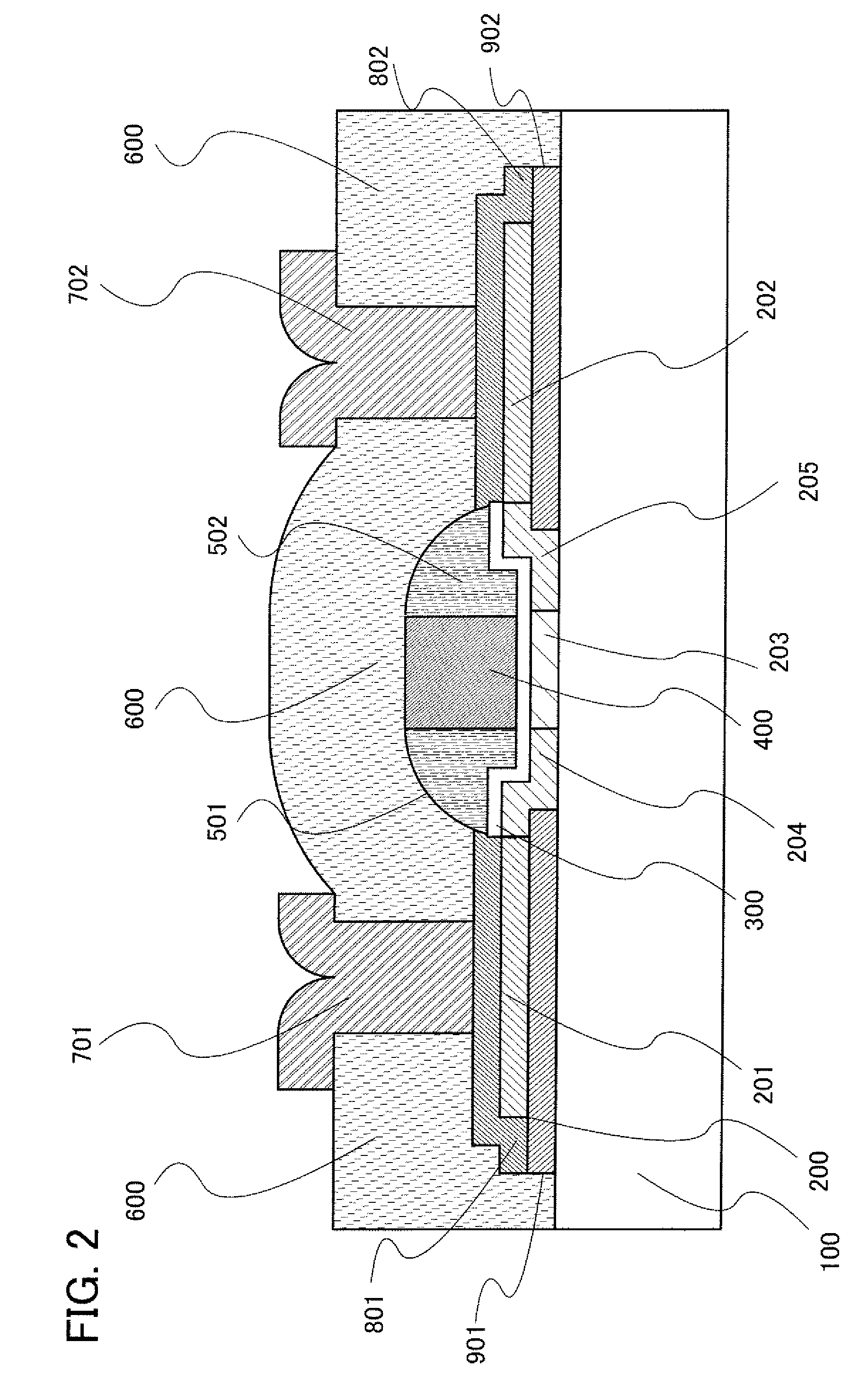
[0110]Semiconductor devices of this embodiment mode are described with reference to FIGS. 2 and 3.

[0111]The semiconductor device of this embodiment mode includes an insulator 100, a semiconductor layer 200 (of an island shape), a gate insulating film 300, a gate electrode 400, a sidewall 501, a sidewall 502, an interlayer insulating film 600, a wiring 701, a wiring 702, an upper electrode 801, an upper electrode 802, a lower electrode 901, and a lower electrode 902 (see FIGS. 2 and 3).

[0112]In the semiconductor device in FIG. 2, the lower electrodes 901 and 902 are formed over the insulator 100.

[0113]The semiconductor device in FIG. 3 has a structure in which opening portions are provided for the insulator 100 (an aperture shape) and a structure in which the lower electrodes 901 and 902 are embedded in the opening portions (an embedded shape).

[0114]The semiconductor layer 200 is formed over the insulator 100 and the lower electrodes 901 and 902.

[0115]The semiconductor layer 200 incl...

embodiment mode 3

[0146]This embodiment mode describes a method for manufacturing the semiconductor device described in Embodiment Mode 1.

[0147]An insulator 100 is provided The insulator may be an insulating substrate or a base insulating film provided over a substrate (see FIG. 4A).

[0148]As the insulating substrate, a glass substrate, a quartz substrate, a resin substrate, or the like can be used.

[0149]As the base insulating film, a single film or stacked films of a silicon oxide film, a silicon nitride film, a silicon nitride oxide film, which contains more nitrogen than oxygen, a silicon oxynitride film, which contains more oxygen than nitrogen, a resin film, and the like can be used.

[0150]Next, a semiconductor film 200a is formed (see FIG. 4B).

[0151]The semiconductor film 200a can be formed using silicon, silicon germanium, or the like by a CVD method, a sputtering method, or the like to have a thickness of 5 to 100 nm.

[0152]Next, crystallization is performed by thermal crystallization, laser cry...


PUM


Abstract

It is an object to provide an element structure of a semiconductor device for having a sufficient contact area between an electrode in contact with a source region or a drain region and the source region or the drain region, and a method for manufacturing the semiconductor device with the element structure. An upper electrode is formed over a high-concentration impurity region (the source region or the drain region). A contact hole passing through an interlayer insulating film is formed overlapping with a region where the upper electrode and the high-concentration impurity region are stacked.

Description

BACKGROUND OF THE INVENTION[0001]1. Field of the Invention[0002]The present invention relates to a semiconductor device including a transistor.[0003]2. Description of the Related Art[0004]A thin film transistor (TFT) is formed using a thin semiconductor layer.[0005]As a method for achieving high performance of a semiconductor device, there is a method which achieves high definition in a semiconductor device. A smaller contact hole is necessary in order to achieve high definition in a semiconductor device.[0006]In order to achieve high performance in a semiconductor device, there is another method in which a channel formation region of a semiconductor layer included in a semiconductor device is thinned.[0007]There is a technology in which increase in field-effect mobility, improvement in a field-effect subthreshold property, and reduction in leak current can be achieved by thinning a channel formation region of a semiconductor layer.[0008]A channel formation region, a source region, ...

Claims


Application Information

Patent Timeline
Patent Type & Authority Patents(United States)
IPC IPC(8): H01L23/48
CPCH01L29/41733H01L29/78621H01L29/66757H01L29/458H01L29/78618
Inventor SHINGU, TAKASHIMATSUKURA, HIDEKI
Owner SEMICON ENERGY LAB CO LTD
Learn More