Structure and method for uniform current distribution in power supply module

Active Publication Date: 2012-10-30
TEXAS INSTR INC
View PDF9 Cites 27 Cited by
  • Summary
  • Abstract
  • Description
  • Claims
  • Application Information

AI Technical Summary

Benefits of technology

[0010]Applicants solved the current crowding problem by depositing an extra metal layer on the top terminal area of the sync FET chip. The selected metal or alloy is preferably copper- or aluminum-based and optionally includes a solderable finish, such as a thin layer of palladium or gold. The thickness of the extra metal layer is selected so that the resistance for a current flowing laterally through the layer area is equal to or less than the resistance for the current, spread over the control chip area, flowing vertically through the control FET chip height. Due to the low lateral resistance, the current will spread approximately uniformly across the bottom terminal before entering the control FET to flow through the chip to the top terminal, enabling the flow of currents between 15 and 30 A without crowding (and without the alternative use of metal clips). Similarly, it is advantageous to deposit an extra metal layer on the top terminal

Problems solved by technology

Applicants observed that the metal clips, which interconnect vertically stacked power FET chips in power supply modules for switching currents between about 10 and 25 A, are poorly suited for customization, since customization emphasizes scalability and time-to-market.
Clips have limited flexibility for shrinking and require long lead times for redesign and re-order.
Furthermore, clips increase the height of the chip stacks and are expensive not only with regard to initial device c

Method used


Image

  • Structure and method for uniform current distribution in power supply module
  • Structure and method for uniform current distribution in power supply module
  • Structure and method for uniform current distribution in power supply module

Examples


Embodiment Construction

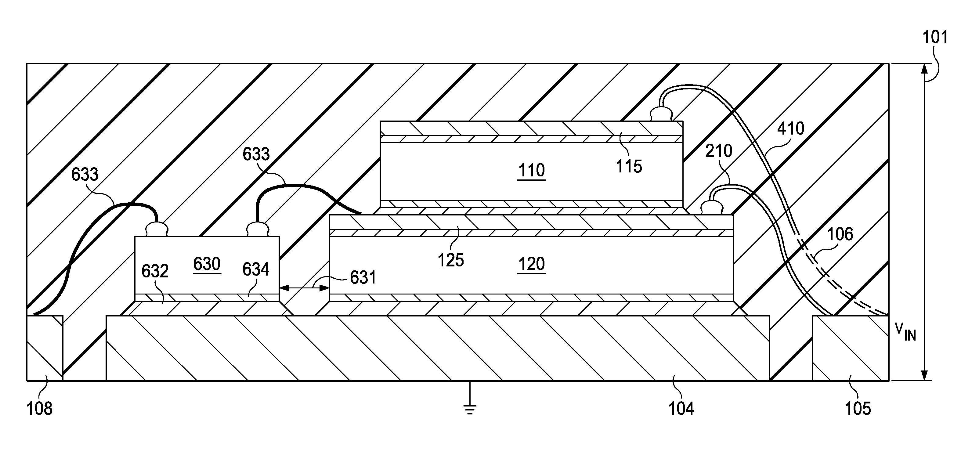
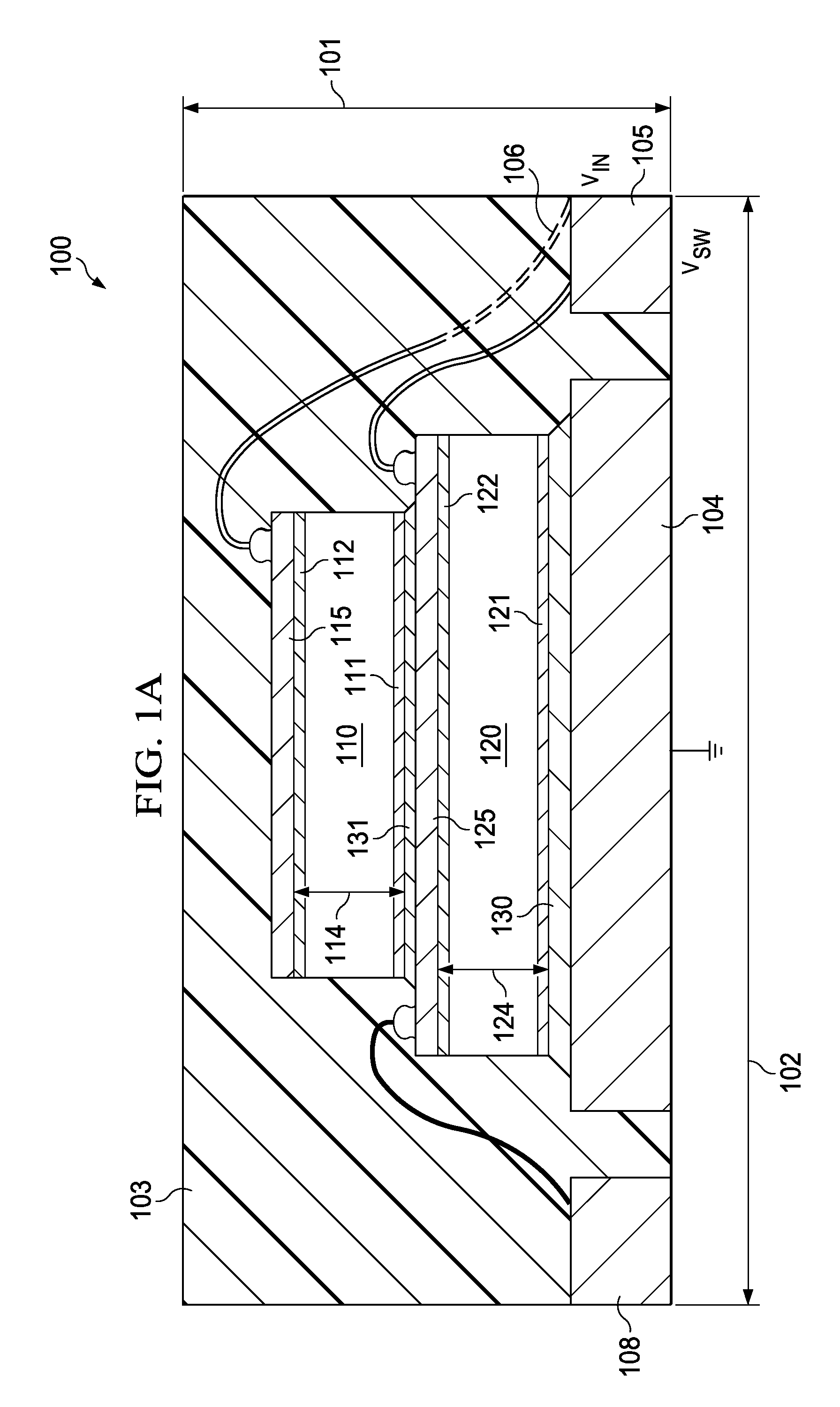
[0031]FIG. 1A illustrates a cross section (simplified and not to scale) of a power supply module generally designated 100 as an exemplary embodiment of the invention. The module dimensions are outlined by encapsulation material 103. A preferred material is an epoxy-based molding compound. The exemplary module of FIG. 1 has a thickness 101 between about 0.8 and 1.0 mm. Consequently, the exemplary module has, due to the lack of metal clips, a smaller thickness than conventional modules with clips (about 1.5 mm thick). It should be noted that design and process improvements under development (such as low-rise wire bonds and thinner chips) will allow a future module thickness of about 0.4 mm. The length 102 of module 100 may be 6 mm, and the width (not shown in FIG. 1A) may be 5 mm. Other modules of the configuration of FIG. 1A may range from 2 by 2 mm to 5 by 7 mm.

[0032]A metal leadframe, generally suitable for Quad Flat No-Lead (QFN) and Small Outline No-Lead (SON) type modules, inclu...


PUM


Abstract

A synchronous Buck converter in a molded package (thickness 101 between 0.8 and 1.0 mm) has vertically assembled control (110) and sync (120) power FET chips and a driver chip (630). The sync chip has one power terminal attached to the leadframe pad (104) and the opposite power terminal covered by a first copper layer (125) connected (210) to a first leadframe terminal (105), the first layer providing a smaller resistance to a current between first terminal and pad than the resistance through the sync chip. The control chip has one power terminal attached to the first layer and the opposite power terminal covered by a second copper layer (115) connected (410) to a second leadframe terminal (106), the second layer providing a smaller resistance to a current from the first to the second terminal than the resistance through the control chip. Connections (210, 410) of layers (125, 115) to leadframe terminals (105, 106) are copper wires of 20 to 50 μm diameter, enabling currents between 3 and 30 A.

Description

FIELD OF THE INVENTION[0001]The present invention is related in general to the field of semiconductor devices and processes, and more specifically to the system structure and fabrication method of a small-size, low cost and scalable power supply system having high efficiency and operating at high frequency and high current.DESCRIPTION OF RELATED ART[0002]Among the popular families of power switching devices are the DC-DC power supply circuits, especially the category of Switched Mode Power Supply circuits. Particularly suitable for the emerging power delivery requirements are the synchronous Buck converters with two power MOS field effect transistors (FETs) connected in series and coupled together by a common switch node. In the Buck converter, the control FET chip, also called the high side switch, is connected between the supply voltage VIN and the LC output filter, and the synchronous (sync) FET chip, also called the low side switch, is connected between the LC output filter and ...

Claims


Application Information

Patent Timeline
IPC IPC(8): H01L23/495
CPCH01L23/49562H01L23/49575H01L23/3107H01L25/16H01L2924/15747H01L2924/30107H01L2924/01047H01L2924/01028H01L2924/01013H01L23/64H01L2924/13091H01L2224/92247H01L2224/73265H01L24/48H01L2224/32145H01L2224/32245H01L2224/45147H01L2224/48137H01L2224/48247H01L2924/00012H01L2924/00H01L2224/45015H01L2924/00014H01L24/45H01L24/73H01L2224/0603H01L2924/181H01L2224/49171H01L24/49H01L2224/49112H01L2224/4903H01L2924/20752H01L2924/20753H01L2924/20755H01L2924/20754H01L2924/2075H01L2224/05599
Inventor TATEISHI, TETSUOROMIG, MATTHEW D
Owner TEXAS INSTR INC
Why Eureka
Try Eureka