Semiconductor device

a technology of semiconductor devices and dielectric devices, applied in semiconductor devices, semiconductor/solid-state device details, electrical apparatus, etc., can solve problems such as destroying the cmos internal circuit, affecting the operation of the device, so as to reduce the interconnection resistance, reduce the interconnection length of the tap interconnection, and increase the permissible value of the current density

Inactive Publication Date: 2013-03-12
RENESAS ELECTRONICS CORP
View PDF5 Cites 11 Cited by
  • Summary
  • Abstract
  • Description
  • Claims
  • Application Information

AI Technical Summary

Benefits of technology

[0027]According to the semiconductor device of the present invention, the two ESD protection elements are respectively connected to the different two nodes in the inductor section. Therefore, there is no need to provide a bridge interconnection connecting between the two ESD protection elements. As a result, an interconnect length of the tap interconnection is reduced.
[0028]According to the present invention, it is possible to reduce an interconnect resistance of a metal interconnection of an ESD discharge path and to increase a permissible value of the current density. Thus, the semiconductor device with excellent ESD protection ability can be achieved.
[0029]Moreover, according to the present invention, it is possible to reduce a formation area of the inductor section and the ESD protection elements.

Problems solved by technology

In particular, impedance mismatch from a desired impedance (50Ω) is caused in a high-frequency region.
Such the voltage stress far exceeds the gate breakdown voltage of 4 V and is large enough to destroy the CMOS internal circuit.
In this case, the metal interconnect path becomes complicated and the metal interconnect length becomes large.
This causes increase in a parasitic resistance of the metal interconnection to each ESD protection element, which results in destruction of the CMOS internal circuit by the voltage increase due to the ESD current.
Moreover, in the case of the configuration shown in FIG. 1, a current density in the discharge path at the time when ESD is applied is high, which causes fusing of a metal interconnection.
Therefore, the current density in the discharge path at the time when ESD is applied becomes higher, which causes fusing of the metal interconnection.
In this case, the metal interconnect path becomes complicated and the metal interconnect length becomes large.
However, the inductor of the T-coil section 10 and the ESD protection element section 20 hardly enjoy the benefit of the miniaturization of the CMOS process.

Method used


Image

  • Semiconductor device
  • Semiconductor device
  • Semiconductor device

Examples


first embodiment

[0045](First Embodiment)

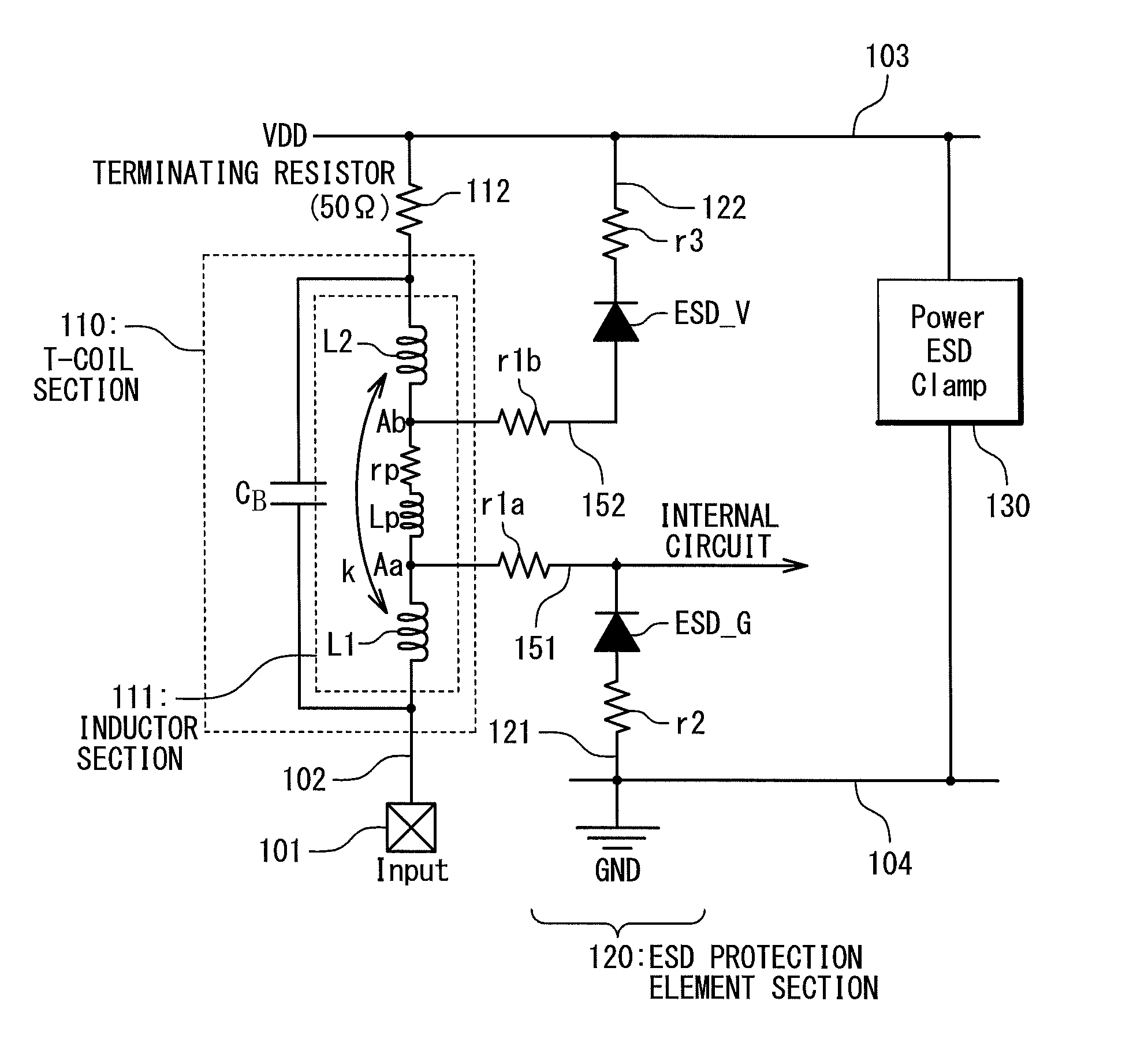
[0046]A semiconductor device according to a first embodiment of the present invention will be described below. FIG. 3 is a circuit diagram showing an interface circuit as the semiconductor device provided with a T-coil and an ESD protection element according to the present embodiment.

[0047]The interface circuit shown in FIG. 3 has a signal input pad 101, a signal line 102, a power supply line 103, a ground line 104, tap interconnections 151 and 152, a T-coil section 110, a terminating resistor 112, an ESD protection element section 120 and a power ESD clamp circuit 130. The power supply line 103 supplies a power supply potential VDD. The ground line 104 supplies a ground potential GND.

[0048]The signal input pad 101 is used for inputting an external signal. The signal line 102 connected to the signal input pad 101 transmits the input signal. The T-coil section 110 has an inductor section 111 and a capacitor CB. The inductor section 111 has an inductor L1 and a...

second embodiment

[0075](Second Embodiment)

[0076]Next, a semiconductor device according to a second embodiment of the present invention will be described. In the second embodiment, a structure in which the semiconductor device described in the first embodiment is placed repeatedly will be described. In this case, the interconnection 121 connected to the GND interconnection 104 and the interconnection 122 connected to the VDD interconnection 103 can be shared by adjacent semiconductor devices. The permissible value of the current density can be increased by enlarging the interconnect widths of the interconnections 121 and 122.

[0077]FIG. 8 is a cross-sectional view showing a structure of the semiconductor device according to the present embodiment. FIGS. 9 and 10 are plan views of the semiconductor device according to the present embodiment. FIG. 9 is a plan view showing a layout of the bottom layer on the substrate shown in FIG. 8. FIG. 10 is a plan view showing a layout of the inductor section 111 in...


PUM


Abstract

A semiconductor device has: a signal pad; a power supply line; a ground line; an inductor section whose one end is connected to the signal pad; a terminating resistor connected between the other end of the inductor section and the power supply line or the ground line. The semiconductor device further has: a first ESD protection element connected to a first node in the inductor section; and a second ESD protection element connected to a second node whose position is different from that of the first node in the inductor section.

Description

INCORPORATION BY REFERENCE[0001]This application is based upon and claims the benefit of priority from Japanese patent application No. 2009-194467, filed on Aug. 25, 2009, the disclosure of which is incorporated herein in its entirety by reference.BACKGROUND OF THE INVENTION[0002]1. Field of the Invention[0003]The present invention relates to a semiconductor device provided with an ESD (ElectroStatic Discharge) protection element.[0004]2. Description of Related Art[0005]An impedance matching technique by using a bridged T-coil is known (refer to, for example, Non-Patent Document 1: “40-Gb / s Amplifier and ESD Protection Circuit in 0.18-μm CMOS Technology”, Sherif Galal, Behzad Razavi, IEEE Journal of Solid-State Circuits VOL. 39, No. 12, pp. 2389-2396, December 2004). In a high-speed interface circuit provided with an ESD protection element, a parasitic capacitance of the ESD protection element and a parasitic capacitance of an input / output circuit affect impedance matching ability. ...

Claims


Application Information

Patent Timeline
Patent Type & Authority Patents(United States)
IPC IPC(8): H01L27/08
CPCH01L23/5227H01L27/0248H01L23/60H01L23/5228H01L2924/3011H01L2924/0002H01L2924/00
Inventor OKUSHIMA, MOTOTSUGUHASHIMOTO, TAKASUKE
Owner RENESAS ELECTRONICS CORP
Why Eureka
Try Eureka