
Microcontact printed thin film capacitors

a thin film capacitor and microcontact technology, applied in the field of multi-layer capacitors, can solve the problems of comparatively large margins, comparatively rough edges on the electrodes, and inability to achieve films with thicknesses, etc., and achieve the comparatively large margins that are required in typical multi-layer capacitors

Inactive Publication Date: 2013-04-09
PENN STATE RES FOUND +1
View PDF276 Cites 5 Cited by
  • Summary
  • Abstract
  • Description
  • Claims
  • Application Information

AI Technical Summary

Benefits of technology

This approach enables the production of multilayer capacitors with high-resolution patterned layers, reducing material waste and processing time, while achieving precise thicknesses and smooth edges, thus enhancing the efficiency and accuracy of capacitor fabrication.

Problems solved by technology

It is uncertain, however, as to whether tape casting can achieve films which have thicknesses of less than 0.2 μm.
This process typically produces comparatively rough edges on the electrodes, which is one factor that leads to the comparatively large margins that are required in typical multilayer capacitors.
Although irradiative lithographic methods may be advantageous for patterning the electrode (and potentially the dielectric) in many circumstances, these methods require sophisticated and expensive apparatus to reproduce a particular pattern on a plurality of substrates.
Additionally, they generally consume more reactants and produce more by-products.
Further, they are relatively time-consuming.

Method used

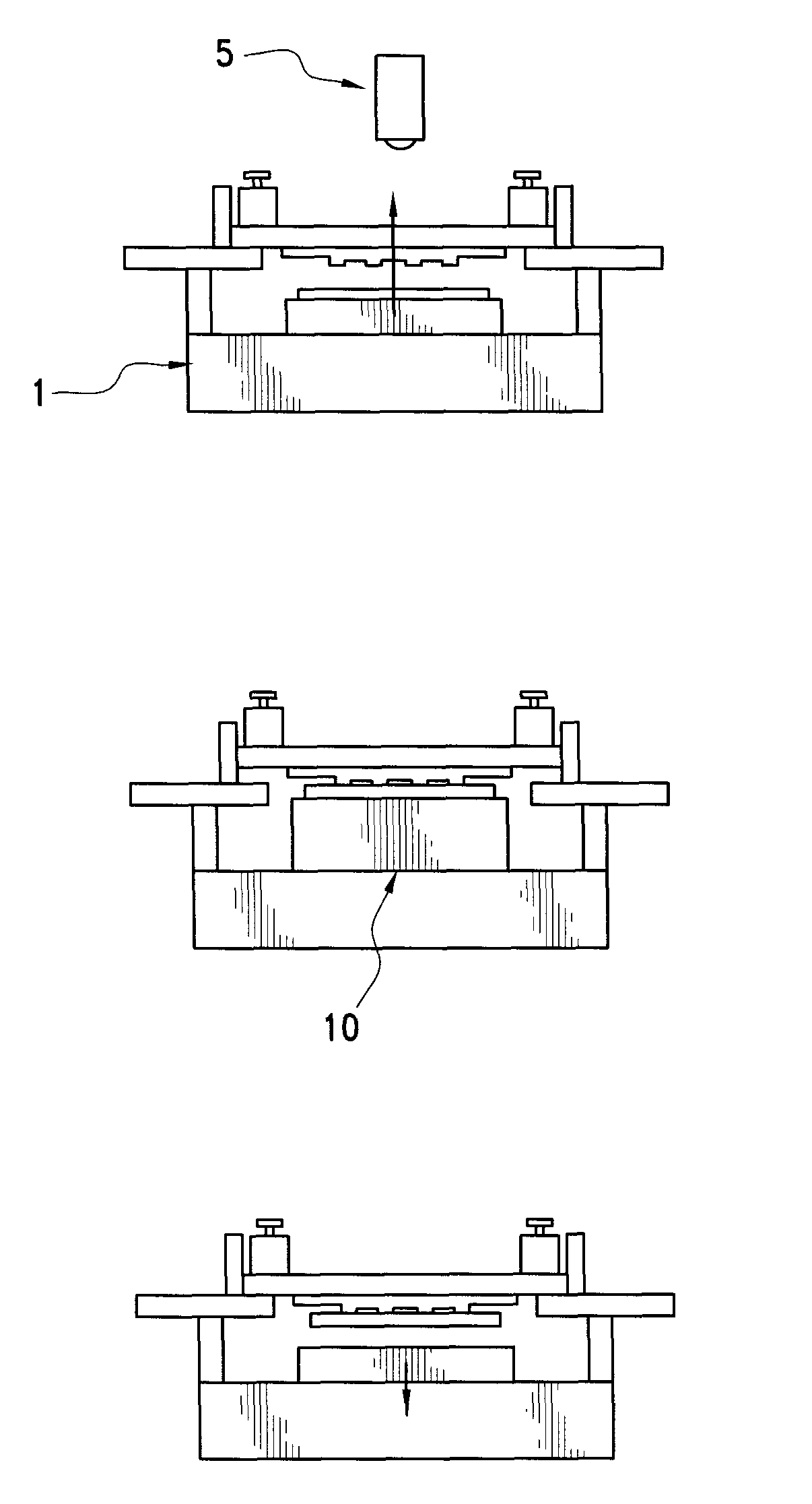
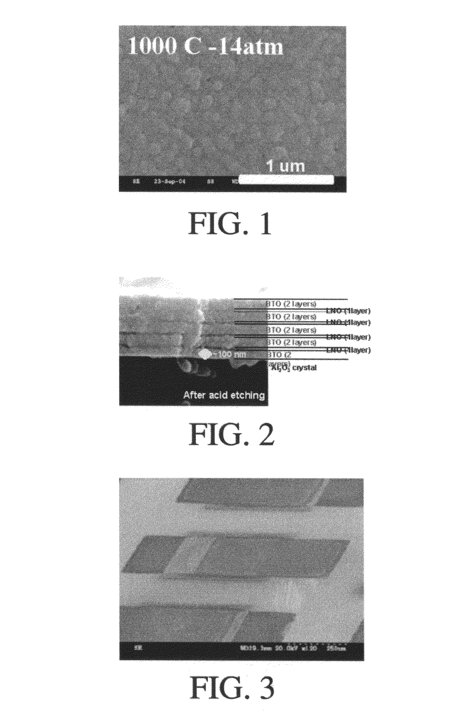
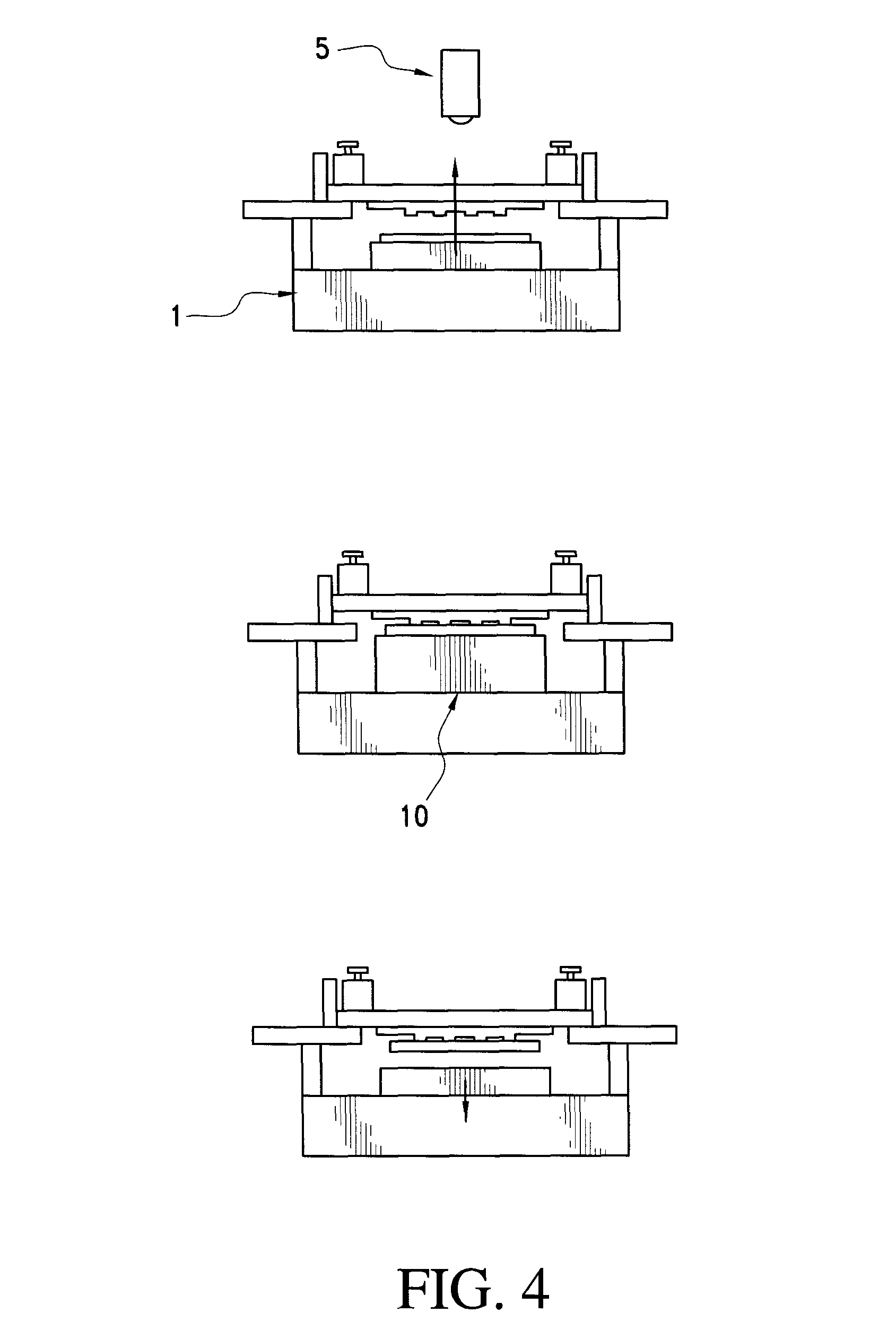

Image

  • Microcontact printed thin film capacitors
  • Microcontact printed thin film capacitors
  • Microcontact printed thin film capacitors

Examples


example 1

Formation of Blanket Thin Film of Stoichiometric BaTiO3 on Ni Foil Substrates by Chemical Solution Deposition

[0039]A Ba precursor solution is made by dissolving 0.01 mol of Ba acetate in 11.74 ml glacial acetic acid. The resulting solution is stirred for 1 hr at 90° C.

[0040]A Ti precursor solution is made by dissolving 0.01 mol of Ti isopropoxide in 2 ml of acetyl acetone.

[0041]A stoichiometric BaTiO3 precursor solution is made by mixing the Ba precursor solution and the Ti precursor solution, and stirring for 1 hr at 90° C. Methanol is added to reduce the stoichiometric BaTiO3 precursor solution molarity to 0.1M.

[0042]The BaTiO3 precursor solution is spin cast at 3000 RPM for 30 sec onto a 99.99% pure Ni foil substrate that is preannealed at 900° C. The film of BaTiO3 precursor solution is dried at 180° C., pyrolyzed at 360° C. and crystallized by rapid thermal annealing at 750° C. This sequence of steps is repeated 8 times to produce a BaTiO3 film thickness of 350 nm. The dielectr...

example 1.1

[0043]The procedure of example 1 is followed except that the sequence of steps is repeated six times to yield a BaTiO3 film thickness of 265 nm. The dielectric constant of the film is 1750 at room temperature and 1600 at 150° C.

example 1.2

[0044]The procedure of example 1 is followed except that the sequence of steps is repeated four times to yield a BaTiO3 film thickness of 173 nm. The dielectric constant of the film is 1300 at room temperature and 1250 at 150° C.


PUM

PropertyMeasurementUnit
thicknessaaaaaaaaaa
thicknessesaaaaaaaaaa
temperatureaaaaaaaaaa

Abstract

The invention relates to thin film single layers, electronic components such as multilayer capacitors which utilize thin film layers, and to their methods of manufacture. Chemical solution deposition and microcontact printing of dielectric and electrode layers are disclosed. High permittivity BaTiO3 multilayer thin film capacitors are prepared on Ni foil substrates by microcontact printing and by chemical solution deposition. Multilayer capacitors with BaTiO3 dielectric layers and LaNiO3 internal electrodes are prepared, enabling dielectric layer thicknesses of 1 μm or less. Microcontact printing of precursor solutions of the dielectric and electrode layers is used.

Description

FIELD OF THE INVENTION[0001]The invention relates to multilayer capacitors and methods for their manufacture.BACKGROUND OF THE INVENTION[0002]The capacitor has substantially shrunk in recent history. Currently, tape casting and related technologies are utilized for the manufacture of multilayer capacitors. There is interest in exploring thin film approaches to creating multilayer capacitors. Ceramic dielectric thin films are commonly formed by a broad range of deposition techniques, such as chemical solution deposition (CSD), evaporation, sputtering, physical vapor deposition and chemical vapor deposition. In order to achieve the requisite dielectric structure, each technique typically requires either a high-temperature deposition or a high-temperature anneal.[0003]Prior art methods of forming a specific structure such as a dielectric that has patterned micron or sub-micron features include irradiative lithographic methods such as photolithography, electron-beam lithography, and x-r...

Claims


Application Information

Patent Timeline
Patent Type & Authority Patents(United States)
IPC IPC(8): B05D5/12
CPCH01G4/1227H01G4/33H01G4/306
Inventor MCKINSTRY, SUSAN TROLIERRANDALL, CLIVE A.NAGATA, HAJIMEPINCELOUP, PASCAL I.BEESON, JAMES J.SKAMSER, DANIEL J.RANDALL, MICHAEL S.TAJUDDIN, AZIZUDDIN
Owner PENN STATE RES FOUND
Learn More