

Multilayer body, piezoelectric element, and liquid ejecting device
a piezoelectric element and multi-layer technology, applied in the field of multi-layer body, piezoelectric element, liquid ejecting device, can solve the problems of unacceptably large surface irregularities, rough surface shape of piezoelectric layer, and inability to obtain desired crystalline phase (e.g., perovskite crystal), so as to achieve the effect of reducing production yield, large surface irregularities, and variability in performance as piezoelectric elements
- Summary
- Abstract
- Description
- Claims
- Application Information
AI Technical Summary
Benefits of technology
Problems solved by technology
Method used
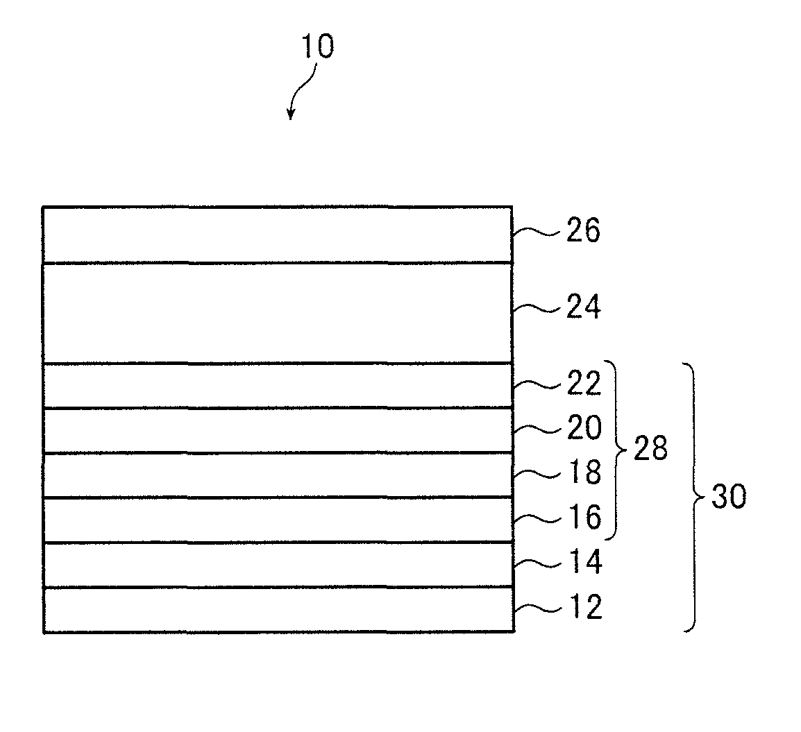
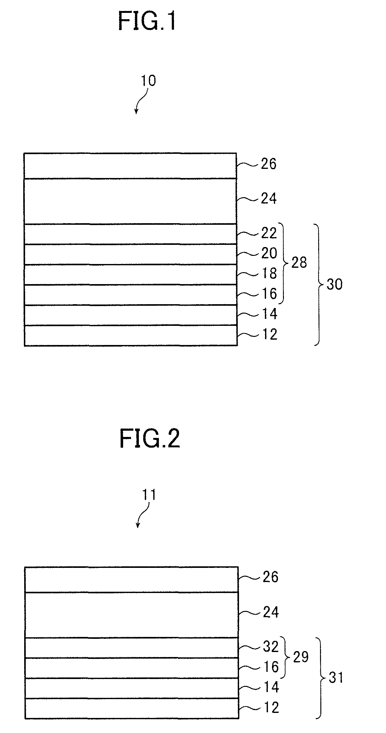
Image

Examples
example 1
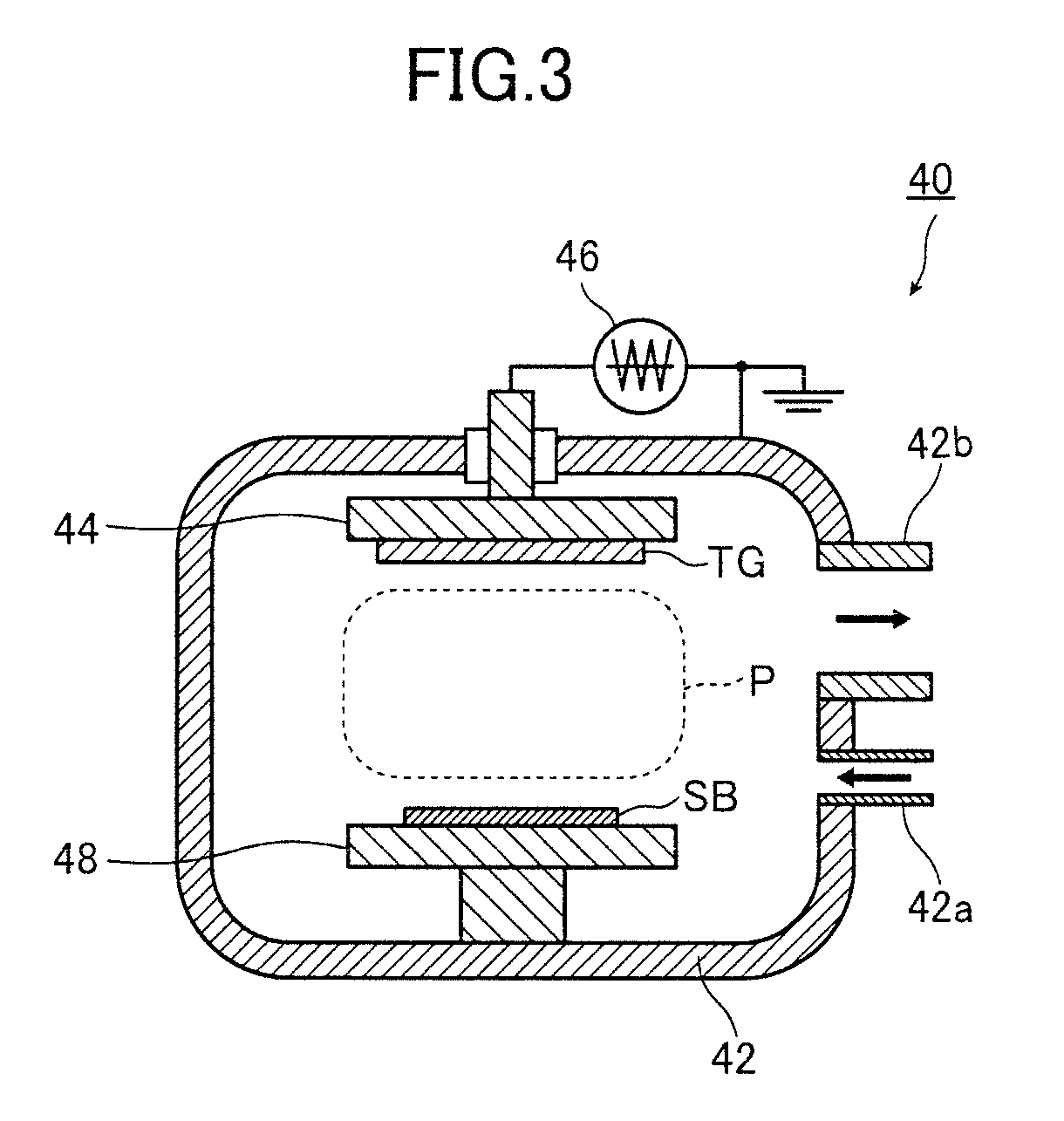
[0204]A model STV4320 sputtering system manufactured by Shinko Seiko Co., Ltd. was used as the sputtering system 40 shown in FIG. 3. In this system 40, either a grounded or floating state may be selected for the substrate holder 48. A high-frequency power supply 46 which is capable of applying a high-frequency power of up to 1 kW was used.
[0205]A substrate having a size of 5 cm square obtained by initially forming a 100 nm thermal oxide film (SiO2 film) on a silicon wafer was used as the substrate SB.
[0206]The distance between the target material TG and the substrate SB was set to 60 mm. Film formation was subsequently carried out at the same distance.
[0207]Using a TiW (tin content, 10 at %) alloy as the target material TG and setting the substrate temperature to 350° C., argon (100%) gas was introduced to the system and a first TiW layer (first adhesive metal sublayer) having a thickness of 20 nm was formed under a pressure of 0.9 Pa.
[0208]Next, a gold-containing sublayer (thicknes...
PUM
| Property | Measurement | Unit |
|---|---|---|
| surface roughness | aaaaa | aaaaa |
| temperature | aaaaa | aaaaa |
| thickness | aaaaa | aaaaa |
Abstract
Description
Claims
Application Information