

Methods for depositing silicon dioxide or silicon oxide films using aminovinylsilanes
a technology of aminovinylsilane and silicon dioxide, which is applied in the direction of crystal growth process, polycrystalline material growth, chemically reactive gas growth, etc., can solve the problem of difficult control of undercut and line width, high etch rate in hf solution, and high etch ra
- Summary
- Abstract
- Description
- Claims
- Application Information
AI Technical Summary
Benefits of technology
Problems solved by technology
Method used
Image

Examples
example 1
The Chemical Compositions of the Film
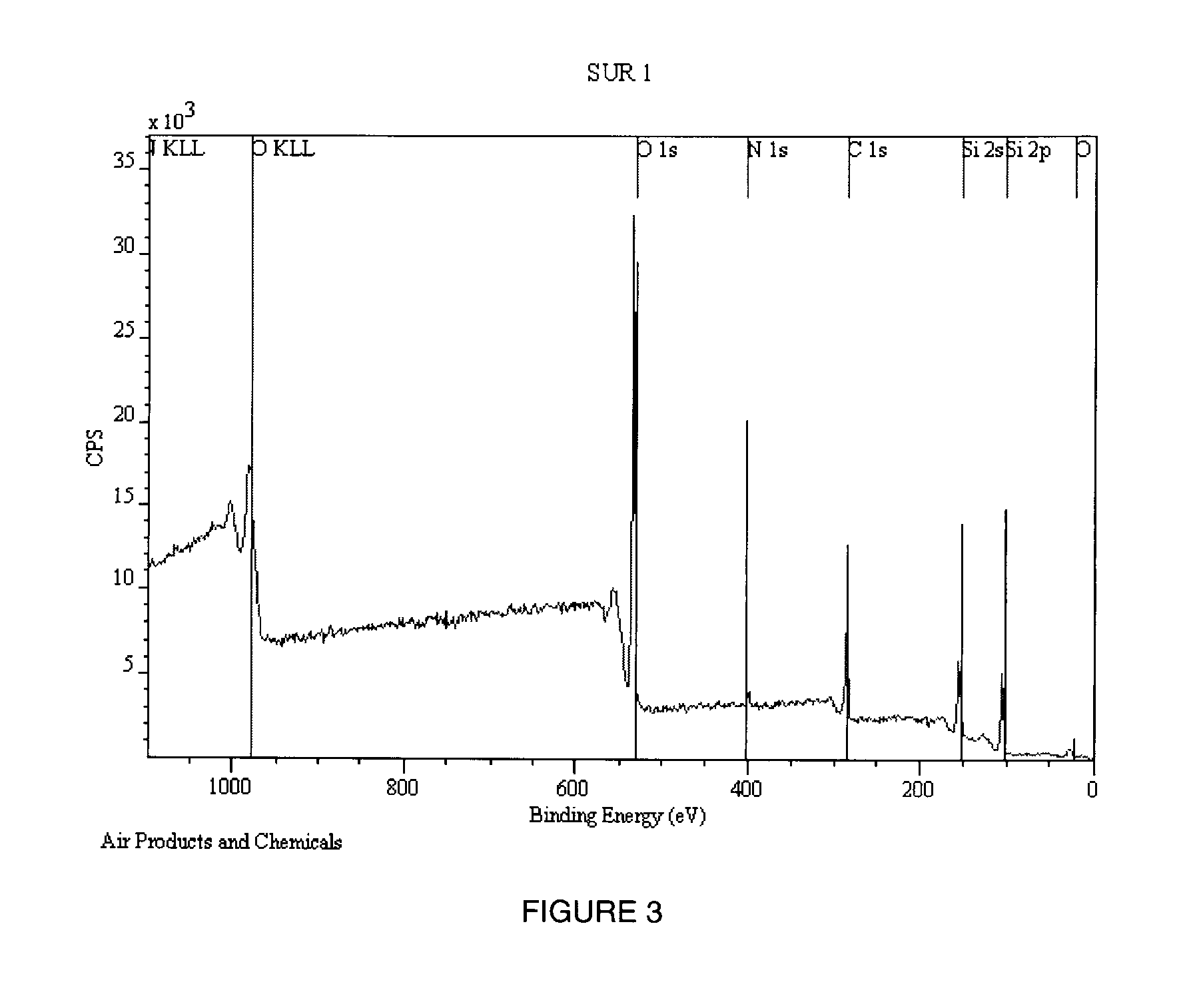
[0087]A typical XPS of the highly uniform nitrogen free films is shown in FIG. 3 and the composition of the different elements including nitrogen is also listed in Table 1. As can be seen from both FIG. 3 and Table 1, no significant nitrogen is detected in the films.
[0088]
TABLE 1Chemical Composition of the Low Etch Rate SiliconDioxide Film (in at %)ElementsOSiCNConcentration70.420.57.91.2
example 2
The Thickness and Etch Rate of the Film
[0089]The silicon dioxide films formed using the said invention are measured for their thickness using an ellisopmeter. The film was etched in a 1 wt % HF solution along with standard thermal silicon dioxide. The etch rate was then calculated from film thickness measurements and compared with that of thermal oxide. The result is listed in Table 2. As can be seen from Table 2, the wet etch rate of the low etch rate SiO2 (Present Invention) is much lower than even thermal oxide film.
[0090]
TABLE 2Wet etch rate of low etch rate SiO2 and standard thermal SiO2 (A / min)After 15 secondAfter 1 minuteAfter 2 minuteMaterialetchetchetchThermal SiO243.227.629.4Low etch SiO21.21.21.2(Present Invention)
example 3
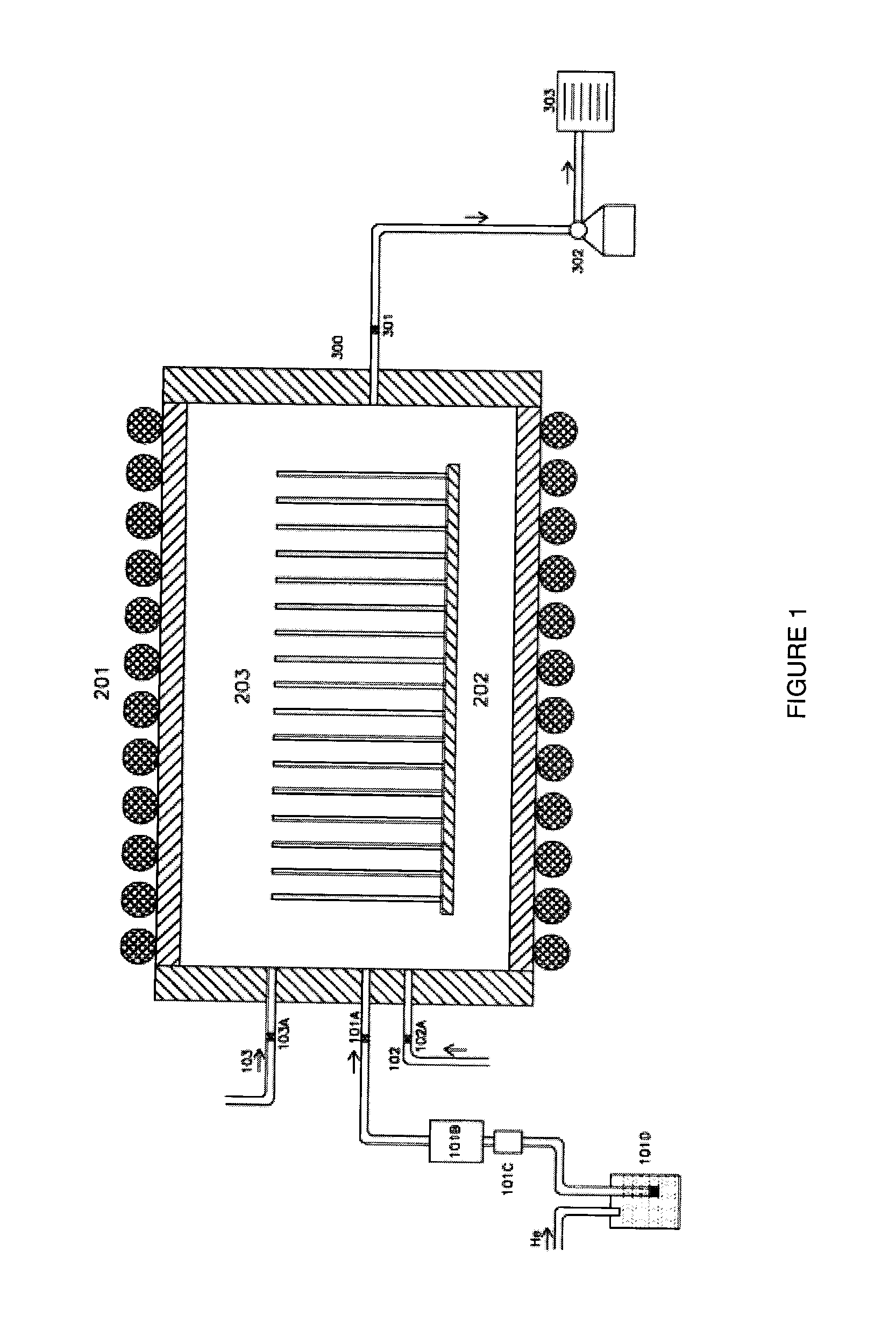
[0091]Using an ATV PE0612 brand low pressure chemical vapor deposition (LPCVD) reactor we loaded twenty five 100 mm Si wafers per deposition run. Upon closing the door to the reactor, we would start the automatic system sequencer to begin the process. The sequence would initially pump the chamber down to a base pressure of ˜1-5 mtorr for about 10 minutes. Then the process would introduce nitrogen purge gas (˜40 to 50 sccm) and begin control the chamber pressure using a throttle valve to obtain the proper process pressure (125 to 500 mtorr.) The process would then ramp the chamber up to the desired process temperature (550° C. or 600° C.), this would take approximately 30 minutes. Upon reaching the process temperature, the wafer temperature was allowed to stabilize for 30 minutes, while still allowing the nitrogen purge gas to flow and maintaining process pressure. After the stabilization period was complete, the nitrogen purge gas flow was shut off and the pr...
PUM
| Property | Measurement | Unit |
|---|---|---|
| temperature | aaaaa | aaaaa |
| pressure | aaaaa | aaaaa |
| temperature | aaaaa | aaaaa |
Abstract
Description
Claims
Application Information