

Semiconductor device and driving method thereof
a technology of magnetic field and driving method, which is applied in the direction of static storage, digital storage, instruments, etc., can solve the problems of high cost per storage capacity, difficult to sufficiently reduce power consumption, short data holding period, etc., and achieves the effect of reducing power consumption, reducing power consumption, and reducing power consumption
- Summary
- Abstract
- Description
- Claims
- Application Information
AI Technical Summary
Benefits of technology
Problems solved by technology
Method used
Image

Examples
embodiment 1
[0087]In this embodiment, a circuit configuration and an operation of a semiconductor device according to one embodiment of the disclosed invention will be described with reference to FIGS. 1A-1, 1A-2, and 1B, FIGS. 2A and 2B, and FIG. 3. Note that in some circuit diagrams mentioned below, “OS” is written beside a transistor in order to indicate that the transistor includes an oxide semiconductor.
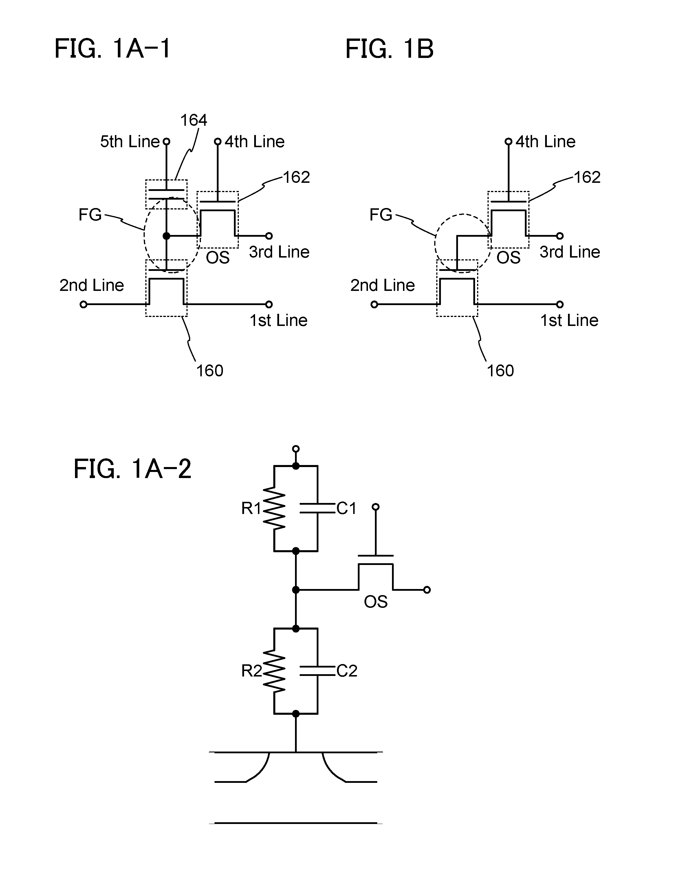
[0088]First, a basic circuit configuration and operation thereof will be described with reference to FIGS. 1A-1, 1A-2, and 1B. In a semiconductor device illustrated in FIG. 1A-1, a first wiring (1st Line) is electrically connected to a drain electrode (or a source electrode) of a transistor 160. A second wiring (2nd Line) is electrically connected to the source electrode (or the drain electrode) of the transistor 160. A third wiring (3rd Line) is electrically connected to a source electrode (or a drain electrode) of a transistor 162. A fourth wiring (4th Line) is electrically connected to a...
application example 1
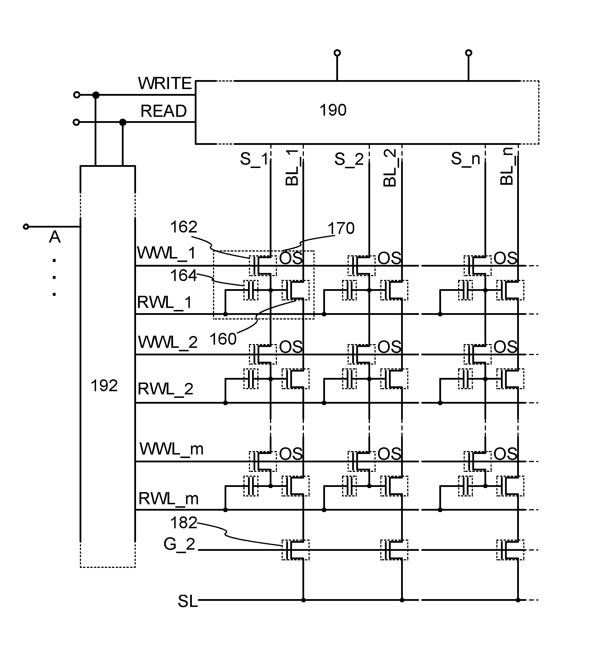
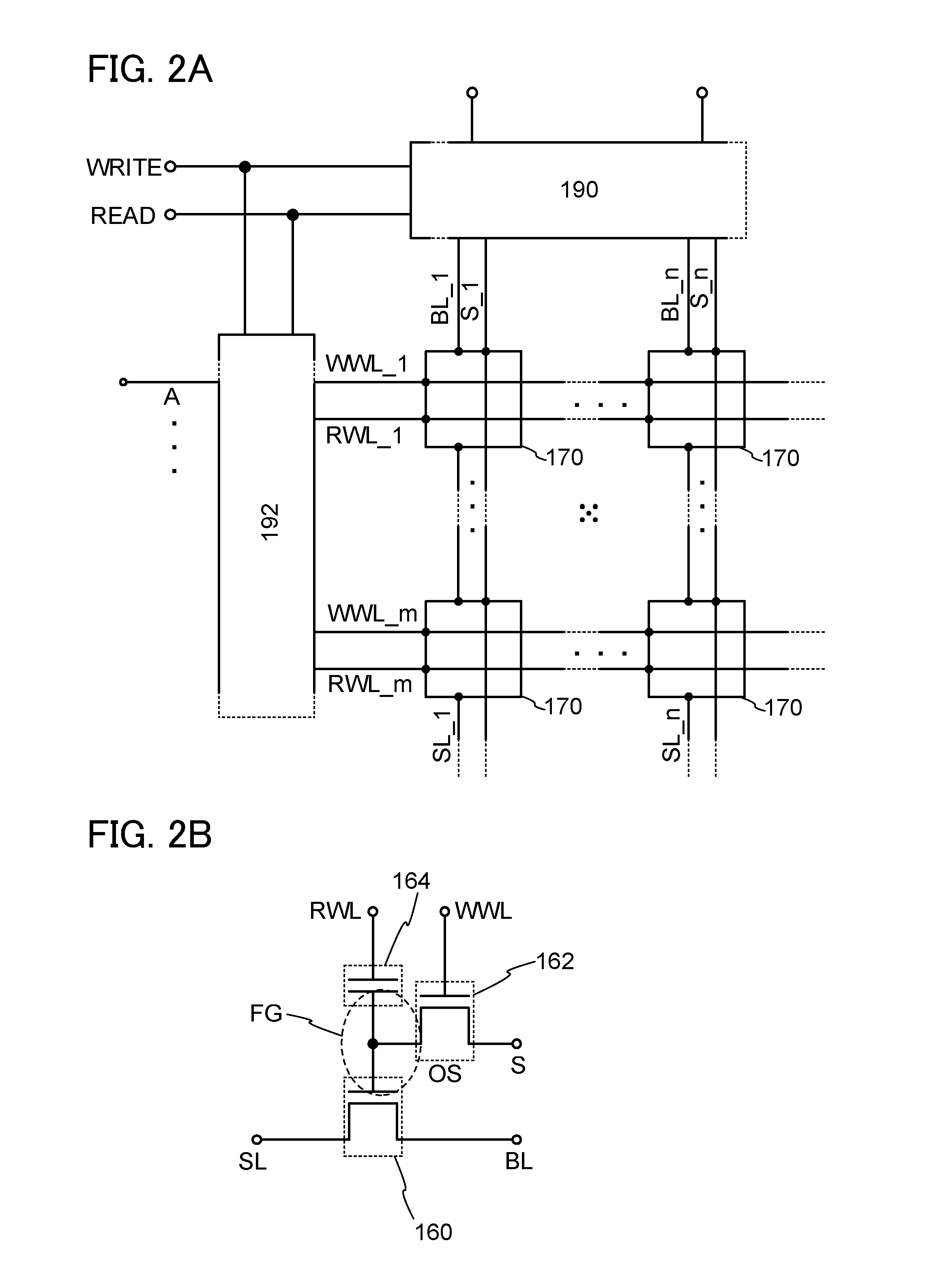
[0114]Next, a more specific circuit structure to which the circuit illustrated in FIGS. 1A-1, 1A-2, and 1B is applied and an operation thereof will be described with reference to FIGS. 2A and 2B and FIG. 3.
[0115]FIG. 2A is an example of a circuit diagram of a semiconductor device including (m×n) memory cells 170. The structure of the memory cells 170 in FIGS. 2A and 2B is similar to that in FIG. 1A-1. That is, as illustrated in FIG. 2B, the first wiring in FIG. 1A-1 corresponds to a bit line BL in FIG. 2B; the second wiring in FIG. 1A-1, a source line SL in FIG. 2B; the third wiring in FIG. 1A-1, a signal line S in FIG. 2B; the fourth wiring in FIG. 1A-1, a write word line WWL in FIG. 2B; and the fifth wiring in FIG. 1A-1, a read word line RWL in FIG. 2B. Note that in FIG. 2A, only the memory cells 170 of the first row are directly connected to the bit lines BL, and only the memory cells 170 of the m-th row are directly connected to the source lines SL. The memory cells 170 of the o...
application example 2
[0156]Next, a circuit structure which is different from the circuit structure illustrated in FIGS. 2A and 2B will be described with reference to FIGS. 7A and 7B.
[0157]FIG. 7A is an example of a circuit diagram of a semiconductor device including (m×n) memory cells 170. The structure of the memory cells 170 in FIG. 7A is similar to that in FIG. 1A-1; therefore, the detailed description thereof is omitted. As illustrated in FIG. 7B, the first wiring in FIG. 1A-1 corresponds to a bit line BL in FIG. 7B; the second wiring in FIG. 1A-1, a source line SL in FIG. 7B; the third wiring in FIG. 1A-1, a signal line S in FIG. 7B; the fourth wiring in FIG. 1A-1, a write word line WWL in FIG. 7B; and the fifth wiring in FIG. 1A-1, a read word line RWL in FIG. 7B. Note that FIG. 7A shows a configuration in which a plurality of transistor 162 is connected in series in a column direction, a plurality of transistors 160 is connected in series in the column direction, and thus a plurality of memory ce...
PUM
 Abstract
Description
Claims
Application Information