Super CMOS devices on a microelectronics system

a microelectronics and super cmos technology, applied in the field of low power and mixed signal analog, logic and memory (alm) devices, can solve the problems of more enclosure contacts in layout implementation, more complications, and more circuit components, and achieve the effects of simple circuit architecture, improved system efficiency, and significant cost and performan

Active Publication Date: 2013-07-02
SCHOTTKY LSI
View PDF30 Cites 19 Cited by
  • Summary
  • Abstract
  • Description
  • Claims
  • Application Information

AI Technical Summary

Benefits of technology

[0008]The disclosed approaches, semiconductor process means, circuit configurations, component and system implementations and manufacturing methods are grouped and classified as the Super CMOS (SCMOS) technology, which offers significant cost and performances, reliability advantages, and improved system efficiency over the conventional CMOS IC approaches. The SCMOS device retains the best part of its predecessors such as the Bipolar Junction Transistor (BJT), the Complementary Metal Oxide Silicon Transistor (CMOST) process and circuit solutions, and creates a super set of macros with new and simpler circuit architecture, static and dynamic operations.
[0009]The application of the SCMOS techniques is not only to crystalline Si devices, which includes mixed signal and various multi-core Si Chips in the Si single crystal substrates, but may also be expanded to include low cost amorphous Si (A-Si) apparatus as well, as well as devices with A-Si, GaAs thin film layers on glass or metal panels, and solar cell and engines. The overall solar energy conversion efficiency can be improved beyond the well known conventional means.

Problems solved by technology

Other circuit components, which have more enclosure contacts in layout implementations, may have more pronounced area impacts.
The device complexity has grown to over billions of circuit elements with complementary MOS (CMOS) constructs.
Still more complications were added to the devices; the Flash transistors as memory blocks, almost doubled in process and mask steps and added complicated circuit manipulations.
The BJT are bulky, have poor transistor yield, and burns DC power.
The CMOS device was slow at the early stage when the thin film was thick.
However, the low cost CMOS sees its own shadow when the PHY scaling is approaches the end by 2012, and the voltage scale down is facing speed degradation when the power supply is below 1.8V for many analog and digital circuits.

Method used


Image

  • Super CMOS devices on a microelectronics system
  • Super CMOS devices on a microelectronics system
  • Super CMOS devices on a microelectronics system

Examples


Embodiment Construction

[0032]The present invention relates generally to the low power and mixed signal analog, logic and memory (ALM) devices in a microelectronics system environment, including the methods of designing and manufacturing certain chip sets, module and PCB sub-assemblies.

[0033]The following description is presented to enable one of ordinary skill in the art to make and use the invention and is provided in the context of a patent application and its requirements. Various modifications to the preferred embodiment and the generic principles and features described herein will be readily apparent to those skilled in the art. Thus, the present invention is not intended to be limited to the embodiment shown but is to be accorded the widest scope consistent with the principles and features described herein.

[0034]Generic IC solution options utilizing mixed analog, logic and memory blocks are proposed with the following ground rules.

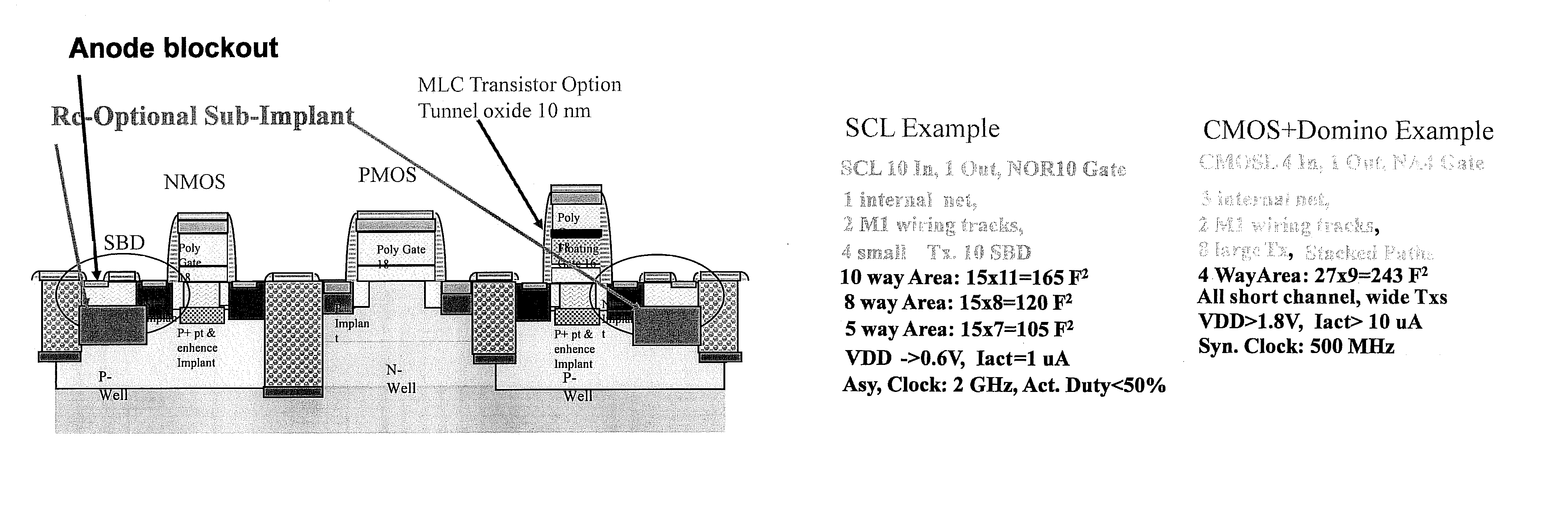
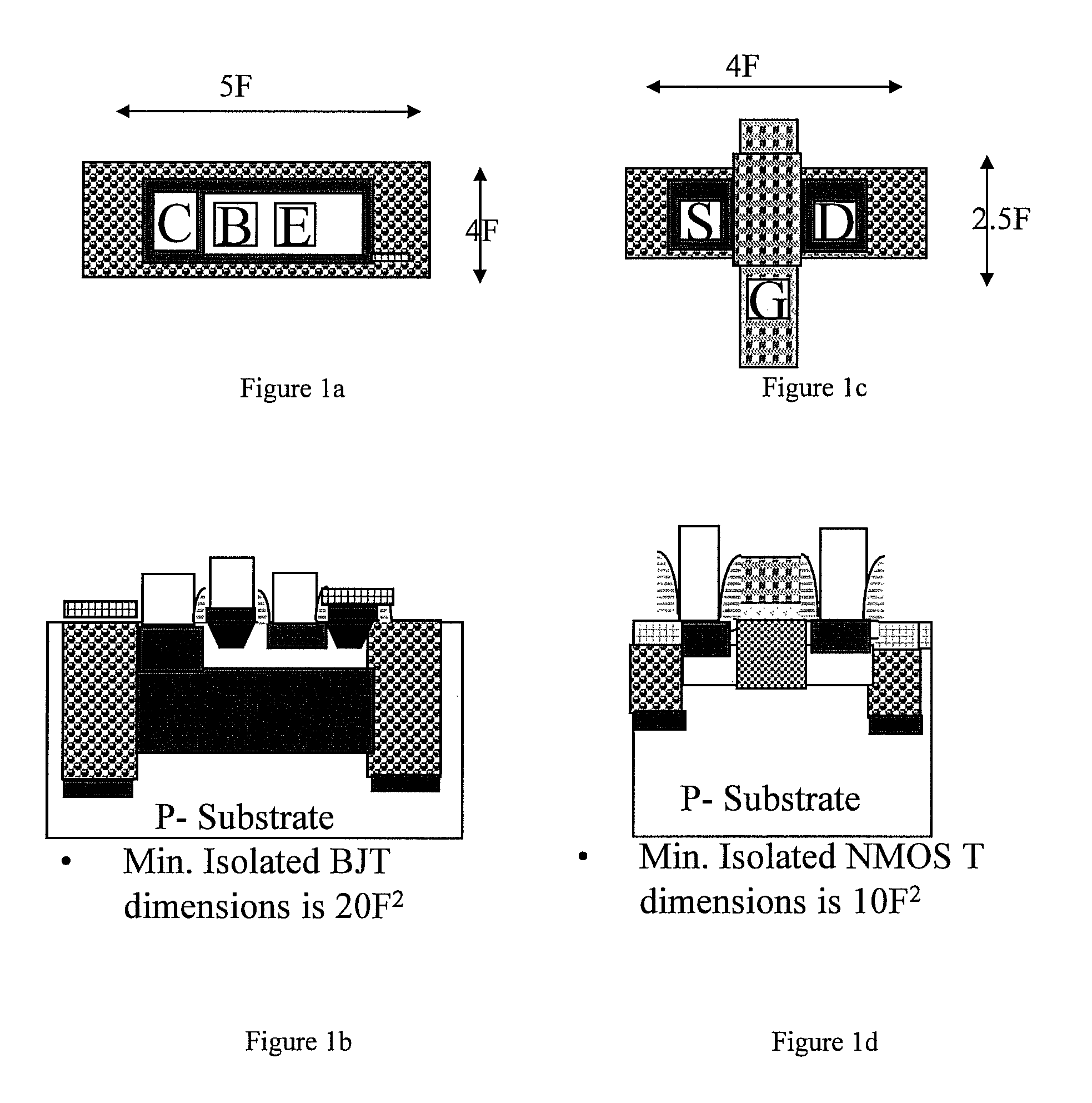
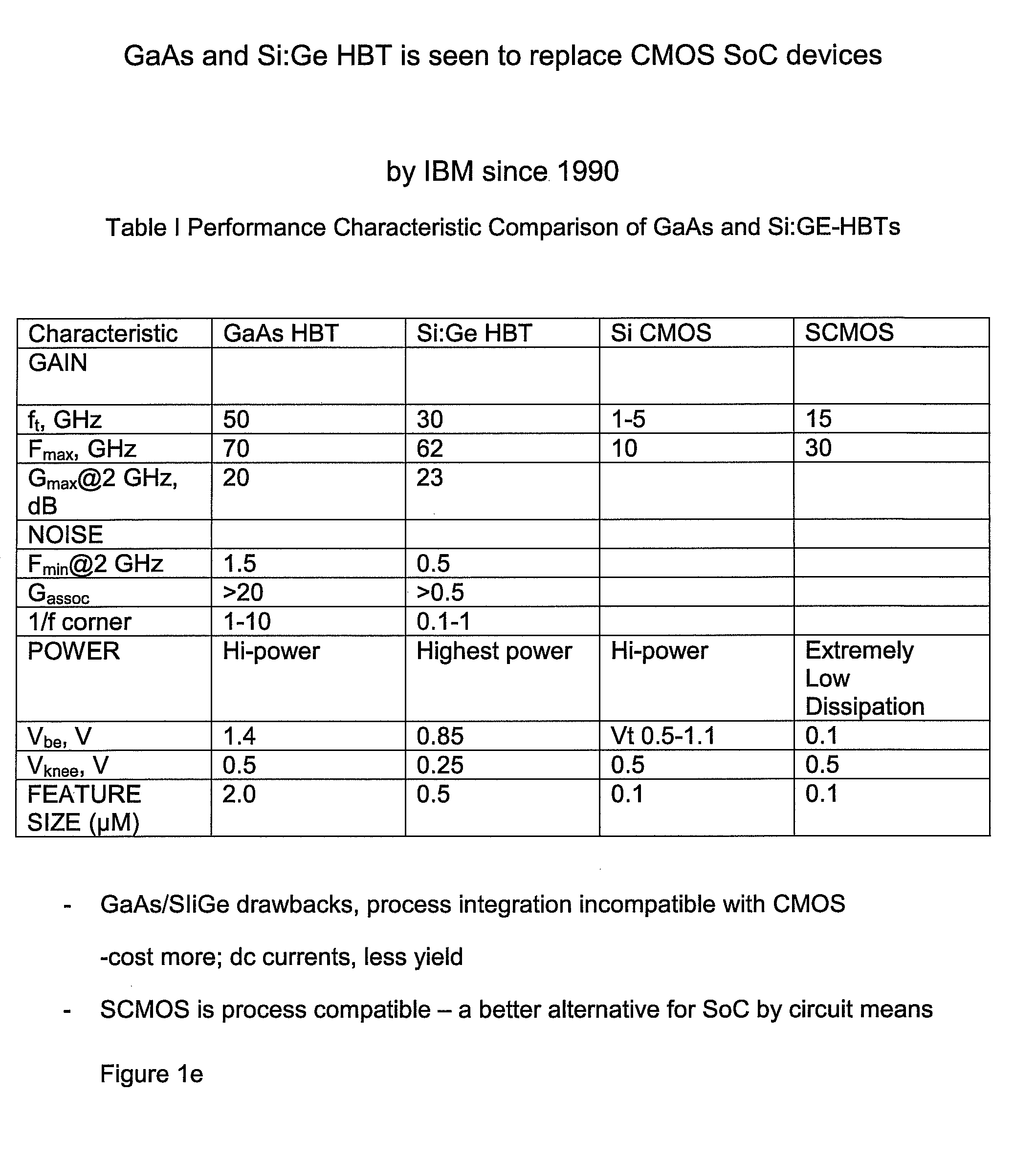
[0035]1. The main emphasis is to utilize the SBD as much as possible ...


PUM


Abstract

A low cost IC solution is disclosed in accordance with an embodiment to provide Super CMOS microelectronics macros. Hereinafter, the Super CMOS or Schottky CMOS all refer to SCMOS. The SCMOS device solutions with a niche circuit element, the complementary low threshold Schottky barrier diode pairs (SBD) made by selected metal barrier contacts (Co / Ti) to P- and N- Si beds of the CMOS transistors. A DTL like new circuit topology and designed wide contents of broad product libraries, which used the integrated SBD and transistors (BJT, CMOS, and Flash versions) as basic components. The macros are composed of diodes that are selectively attached to the diffusion bed of the transistors, configuring them to form generic logic gates, memory cores, and analog functional blocks from simple to the complicated, from discrete components to all grades of VLSI chips. Solar photon voltaic electricity conversion and bio-lab-on-a-chip are two newly extended fields of the SCMOS IC applications.

Description

FIELD OF THE INVENTION[0001]The present invention relates generally to the low power and mixed signal analog, logic and memory (ALM) devices in a microelectronics system environment, including the methods of designing and manufacturing certain chip sets, module and PCB sub-assemblies.BACKGROUND OF THE INVENTION[0002]Since the introduction of the IC devices, workers have been trying to increase the IC density, and reduce the cost of manufacturing chips. The first approach means to put more components / functionality onto a chip. The second approach is to build more chips on a larger substrate. The substrate Si wafer processing facility has grown from 2.5 IN diameter to 12 IN. One wafer may hold 10 k full dices to reduce the unit costs. A common need to serve both purposes well is to reduce the physical dimensions of each circuit's elements.[0003]Various attempts were tried in the past to improve IC functionality, performance, and cost figures. The early IC implementations were done via...

Claims


Application Information

Patent Timeline
Patent Type & Authority Patents(United States)
IPC IPC(8): H01L27/092H01L27/095
CPCH01L27/0207H03K19/17728H01L27/105H01L27/10897H01L27/112H01L27/11253H01L27/11286H01L27/11526H01L27/11546H01L27/11807H01L31/032H01L31/0376H01L31/072H01L31/074H01L27/0727H01L28/20Y02E10/50H01L2924/0002Y02E10/548H10B12/50H10B20/38H10B20/60H10B20/00H10B41/49H10B41/40H01L2924/00H10B20/65H01L25/065H01L21/8238H01L27/0629H01L29/66143H01L29/872H01L31/03762H01L31/07
Inventor CHANG, AUGUSTINE WEI-CHUN
Owner SCHOTTKY LSI
Why Eureka
Try Eureka