Fabrication method for surrounding gate silicon nanowire transistor with air as spacers

a silicon nanowire transistor and spacer technology, applied in the field of ultra-large-scale integrated circuit fabrication technology, can solve the problems of severe influence on the transient response of the device, no report on the optimization of parasitic capacitance in the device,

Active Publication Date: 2013-08-20
SEMICON MFG INT (SHANGHAI) CORP +1
View PDF9 Cites 10 Cited by
  • Summary
  • Abstract
  • Description
  • Claims
  • Application Information

AI Technical Summary

Benefits of technology

[0041]The invention has the following advantageous effects in that, the fabrication method for a surrounding gate silicon nanowire transistor with air as spacers according to the invention is compatible with the CMOS process flow. The introduction of the air spacers can effectively reduce the parasitic capacitance of the device, and improve the transient response of the device, so that the method is applicable for a logic circuit with high performance.
in that, the fabrication method for a surrounding gate silicon nanowire transistor with air as spacers according to the invention is compatible with the CMOS process flow. The introduction of the air spacers can effectively reduce the parasitic capacitance of the device, and improve the transient response of the device, so that the method is applicable for a logic circuit with high performance.

Problems solved by technology

However, its parasitic capacitance, especially a fringing parasitic capacitance between a gate and a source / drain (FIG. 1), may not shrink correspondingly, which accounts for an increasing proportion in the total capacitance, resulting in a severe influence on the transient response of the device.
However, there is no report on the optimization for parasitic capacitance in this device.

Method used


Image

  • Fabrication method for surrounding gate silicon nanowire transistor with air as spacers
  • Fabrication method for surrounding gate silicon nanowire transistor with air as spacers
  • Fabrication method for surrounding gate silicon nanowire transistor with air as spacers

Examples


embodiment 1

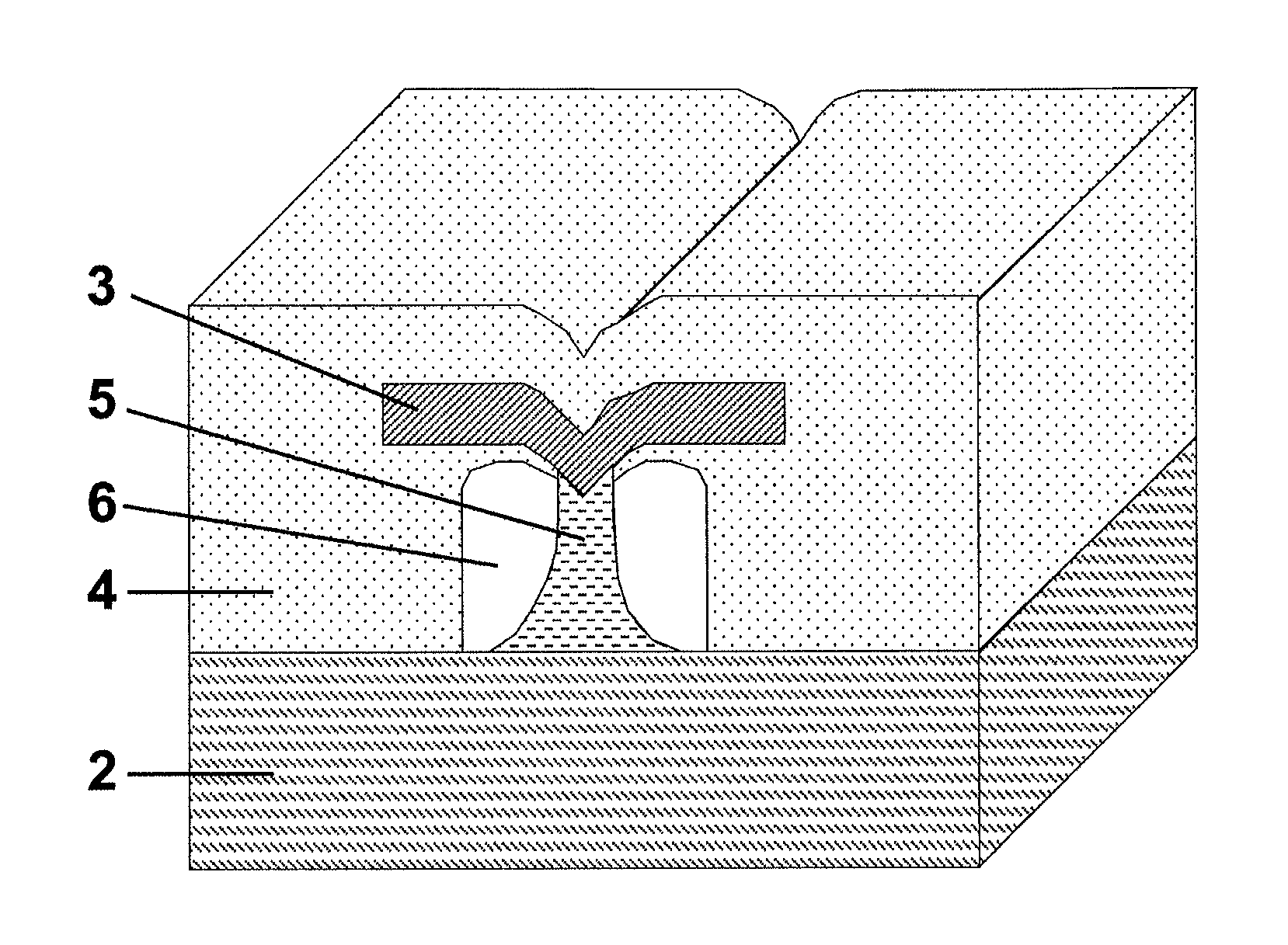
[0051]starting from a SOI substrate (Si having a thickness of 2500 Å on a buried oxide layer), sequentially performing the following steps:

[0052]1. A silicon island isolation method is adopted;

[0053]2. A SiN 3 with a thickness of 1500 Å is deposited by using a low pressure chemical vapor deposition (LPCVD);

[0054]3. Photolithography is performed to define a Fin hard mask;

[0055]4. The SiN 3 is etched by 1500 Å through a reactive ion etching (RIE) technology, and then the photoresist is removed by cleaning, as shown in FIG. 7;

[0056]5. An As implantation is performed with a 0° angle, an energy of 50 KeV, and a dosage of 4×1015 cm−2, as shown in FIG. 8;

[0057]6. A photolithography is performed to define a channel region and large source / drain regions;

[0058]7. The Si 1 is etched by 2500 Å through inductively coupled plasma (ICP), by using the photoresist and the SiN Fin hard mask as barriers, so that the Fin and the large source / drain are formed, and is then cleaned to remove the photoresi...

embodiment 2

[0079]as compared with embodiment 1, the difference is in the following steps:

[0080]1. A LOCOS isolation method is used;

[0081]2. A SiO2 with a thickness of 1500 Å is deposited by using a low pressure chemical vapor deposition (LPCVD);

[0082]4. The SiO2 is etched by 1500 Å through a reactive ion etching (RIE) technology, and the photoresist is removed by cleaning;

[0083]7. The Si is etched by 2500 Å through inductively coupled plasma (ICP), using the photoresist and the SiO2 Fin hard mask as barriers, so that the Fin and the large source / drain are formed, and then the photoresist is removed by cleaning;

[0084]8. The SiO2 is selectively etched by a buffered hydrofluoric acid (BHF) at 170° C., and the SiO2 hard mask is completely removed;

[0085]9. A wet oxidation is performed to form a silicon nanowire;

[0086]10. The SiO2 formed by wet oxidation is etched by a buffered hydrofluoric acid (BHF) to form a floating silicon nanowire.


PUM

PropertyMeasurementUnit
thicknessaaaaaaaaaa
angleaaaaaaaaaa
thicknessaaaaaaaaaa

Abstract

The invention discloses a fabrication method for a surrounding gate silicon nanowire transistor with air as spacers. The method comprises: performing isolation, and depositing a material A which has a higher etch selectivity ratio with respect to Si; performing photolithography to define a Fin hard mask; etching the material A to form the Fin hard mask; performing source and drain implantation; performing photolithography to define a channel region and large source / drain regions; forming the Si Fin and the large source / drains; removing the hard mask of the material A; forming a nanowire; etching the SiO2 to form a floating nanowire; forming a gate oxide layer; depositing a polysilicon; performing polysilicon injection; performing annealing to activate dopants; etching the polysilicon; depositing SiN; performing photolithography to define a gate pattern; etching the SiN and the polysilicon to form the gate pattern; separating the gate and the source / drain with a space in between filled with air; depositing SiO2 to form air sidewalls; performing annealing to densify the SiO2 layer; using subsequent processes to complete the device fabrication. The invention is compatible with the CMOS process flow. The introduction of the air sidewalls can effectively reduce the parasitic capacitance of the device, and improve the transient response of the device, so that the method is applicable for a logic circuit with high performance.

Description

CROSS-REFERENCE TO RELATED APPLICATION[0001]The present application is a U.S. National Stage application of PCT application (PCT / CN2011 / 077213). The PCT application claims priority to Chinese Patent Application (No. 201110139453.9) filed on May 26, 2011, which is incorporated herein by reference in its entirety as if set forth herein.FIELD OF THE INVENTION[0002]The invention refers to a field of ultra large scale integrated (ULSI) circuit fabrication technology, particularly relates to a fabrication method for a surrounding gate silicon nanowire transistor with air as spacers.BACKGROUND OF THE INVENTION[0003]As the feature size of a CMOS device gradually shrinks, it enters into a deep submicron and a nanometer regime. However, its parasitic capacitance, especially a fringing parasitic capacitance between a gate and a source / drain (FIG. 1), may not shrink correspondingly, which accounts for an increasing proportion in the total capacitance, resulting in a severe influence on the tran...

Claims


Application Information

Patent Timeline
Patent Type & Authority Patents(United States)
IPC IPC(8): H01L21/84
CPCH01L29/66439B82Y10/00H01L29/775
Inventor HUANG, RUZHUGE, JINGFAN, JIEWENAI, YUJIEWANG, RUNSHENGHUANG, XIN
Owner SEMICON MFG INT (SHANGHAI) CORP
Why Eureka
Try Eureka