Apparatus and method of substrate to substrate bonding for three dimensional (3D) IC interconnects

a three-dimensional, interconnected technology, applied in the direction of coupling device connection, auxillary welding device, soldering apparatus, etc., can solve the problems of structural and electrical defects, adversely affect the performance of the device, and low k materials are typically porous materials that may not be mechanically robust as traditional dielectrics, so as to improve the mechanical robustness of traditional dielectrics, reduce the cost of manufacturing, and reduce the effect of k materials

Active Publication Date: 2013-09-10
TAIWAN SEMICON MFG CO LTD
View PDF10 Cites 1 Cited by
  • Summary
  • Abstract
  • Description
  • Claims
  • Application Information

AI Technical Summary

Benefits of technology

[0010]One advantage for an illustrative embodiment is that the bonding apparatus may require a lower bonding temperature than the conventional process of plasma pre-treatment followed by transport to a conventional bonding tool. Further, a less aggressive, therefore less damaging plasma pre-treatment is implemented. The undamaged low k materials will result in an improved RC delay time. Moreover, a reduced processing time, due to the lower temperature, may also be an advantage.
[0011]An additional advantage is that the gap of the two substrates of the resulting bonded metal pads may be reduced to less than about 5 μm, preferably less than about 1 μm. The benefit of reducing the gap to less than 5 μm is the reduction of moisture penetrating the gap material and corroding the metal pads. Further, a thinner gap may ease the complexity of further processing the bonded substrates.

Problems solved by technology

Conventional direct metal bonding may cause structural and electrical defects when employed for Cu to Cu bonding on structures that comprise a low k dielectric.
As semiconductor chips have scaled, the insulating dielectrics between metal layers have thinned to the point where charge build up and crosstalk adversely affect the performance of the device.
However, low k materials are typically porous materials that may not be as mechanically robust as traditional dielectrics.
The surface oxides and contamination may begin to accumulate on the metal surfaces of the substrates.
Further, the metal bond pads are exposed to atmosphere in the conventional bonding tool.
A disadvantage of the conventional direct metal bonding is that an additional plasma pre-treatment may damage the device or low k material.
Additionally, the relatively high temperature of the conventional bonding may further damage low k material.
Damaged low k material may have a higher dielectric constant and thus result in higher RC delay for the 3D device.
A further disadvantage of the conventional direct metal bonding is that the surfaces of the metal pads may have a gap separating them that has a thickness of between about 20-40 μm in a solder ball process.
This oxide and / or contamination layer may be porous and moisture may then corrode the metal pads, causing device reliability problems.

Method used


Image

  • Apparatus and method of substrate to substrate bonding for three dimensional (3D) IC interconnects
  • Apparatus and method of substrate to substrate bonding for three dimensional (3D) IC interconnects
  • Apparatus and method of substrate to substrate bonding for three dimensional (3D) IC interconnects

Examples


Embodiment Construction

[0020]The making and using of the presently preferred embodiments are discussed in detail below. It should be appreciated, however, that an illustrative embodiment provides many applicable inventive concepts that can be embodied in a wide variety of specific contexts. The specific embodiments discussed are merely illustrative of specific ways to make and use the invention, and do not limit the scope of the invention.

[0021]An advantage of an illustrative embodiment is that the illustrative embodiment provides a 3D IC with little or no low k damage, and a small gap thickness between the first and second substrate. The gap, according to an illustrative embodiment, may be between less than 1 μm to 5 μms.

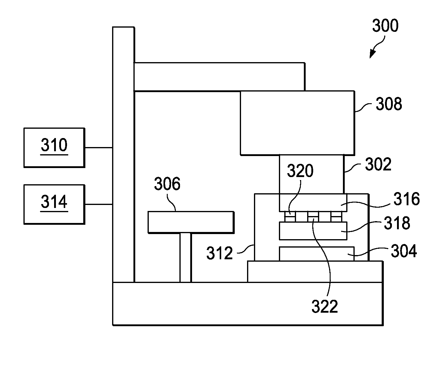
[0022]FIG. 1 is a cross sectional depiction of a three dimensional semiconductor integrated circuit (3D IC) interconnect formed by a direct metal bonding process. In this example, first substrate 102 may be comprised of a semiconductor wafer, semiconductor die, other substrate, flip-chip...


PUM

PropertyMeasurementUnit
pressureaaaaaaaaaa
temperatureaaaaaaaaaa

Abstract

An apparatus including a bond head, a supplemental support, a reduction module, and a transducer is provided. The bond head holds a first substrate that contains a first set of metal pads. The supplemental support holds a second substrate that contains a second set of metal pads. The aligner forms an aligned set of metal pads by aligning the first substrate to the second substrate. The reduction module contains the aligned substrates and a reduction gas flows into the reduction module. The transducer provides repeated relative motion to the aligned set of metal pads.

Description

TECHNICAL FIELD[0001]The present invention relates generally to an apparatus and a method of substrate to substrate bonding for a three dimensional interconnect and, in particular, to an apparatus and a method of direct metal bonding.BACKGROUND[0002]As the cost of shrinking semiconductor devices continues to increase, alternative approaches, such as extending the integration of circuits into the third dimension or semiconductor substrate stacking, are being explored. Two or more substrates are bonded together to form a three dimensional structure. Several bonding processes have been implemented for these structures.[0003]Adhesive bonding and dielectric fusion bonding are bonding processes that bond dielectric layers together. Adhesive bonding and dielectric fusion bonding are typically used in processes that require further processing steps after bonding, such as through via etch processes. Conventional direct metal bonding is another method of bonding that bonds metal from one subs...

Claims


Application Information

Patent Timeline
Patent Type & Authority Patents(United States)
IPC IPC(8): B23K1/06B23K31/02
CPCH01L24/64H01L24/75H01L24/81H01L2924/01082H01L2924/01019H01L2924/0105H01L2224/75301H01L2224/81054H01L24/16H01L2224/751H01L24/13H01L2924/14H01L2924/30105Y10T29/53174H01L2924/01079H01L2924/01029H01L2224/81894H01L2224/75H01L2224/81205H01L2224/81011H01L2924/01006H01L2224/81801H01L2924/01033H01L2924/01013H01L2924/01075H01L2924/00014H01L2224/056B23K1/06
Inventor YU, CHEN-HUACHIOU, WEN-CHIHWU, WENG-JIN
Owner TAIWAN SEMICON MFG CO LTD
Why Eureka
Try Eureka