Top gate thin film transistor and display apparatus including the same

a technology of thin film transistor and display apparatus, which is applied in the direction of transistors, electrical devices, semiconductor devices, etc., can solve the problems of low heat resistance, difficult to employ flexible substrates, plastic substrates or film substrates, etc., and achieve the effect of suppressing the reduction of resistance in the channel region

Active Publication Date: 2014-01-07
CANON KK
View PDF28 Cites 78 Cited by
  • Summary
  • Abstract
  • Description
  • Claims
  • Application Information

AI Technical Summary

Benefits of technology

[0011]It is therefore an object of the present invention to provide a top gate oxide semiconductor TFT, which is capable of suppressing reduction in resistance of a channel region of an oxide semiconductor layer due to hydrogen diffusion, and to provide a display apparatus including the top gate oxide semiconductor TFT.
[0013]According to the present invention, even in a case where deposition of the protective layer containing hydrogen or hydrogen plasma processing is carried out, it is possible to suppress the reduction in resistance of the channel region made of an oxide semiconductor. Further, by employing the gate electrode layer of the present invention, a leakage current density of the gate insulating layer may be reduced.

Problems solved by technology

However, the manufacture of those TFTs requires a high temperature process, and hence it is difficult to employ a flexible substrate such as a plastic substrate or a film substrate which is low in heat resistance.
However, the increase in thickness of the gate insulating layer may cause an increase in drive voltage of the TFT, or lowering of an on-current or deterioration of an S value.
Further, even when a polycrystalline oxide semiconductor such as indium tin oxide (ITO) and ZnO is used for the gate electrode layer, hydrogen is diffused through grain boundaries in the polycrystalline oxide semiconductor, and hence the reduction in resistance of the channel region of the semiconductor layer cannot be suppressed.

Method used


Image

  • Top gate thin film transistor and display apparatus including the same
  • Top gate thin film transistor and display apparatus including the same
  • Top gate thin film transistor and display apparatus including the same

Examples


example 1

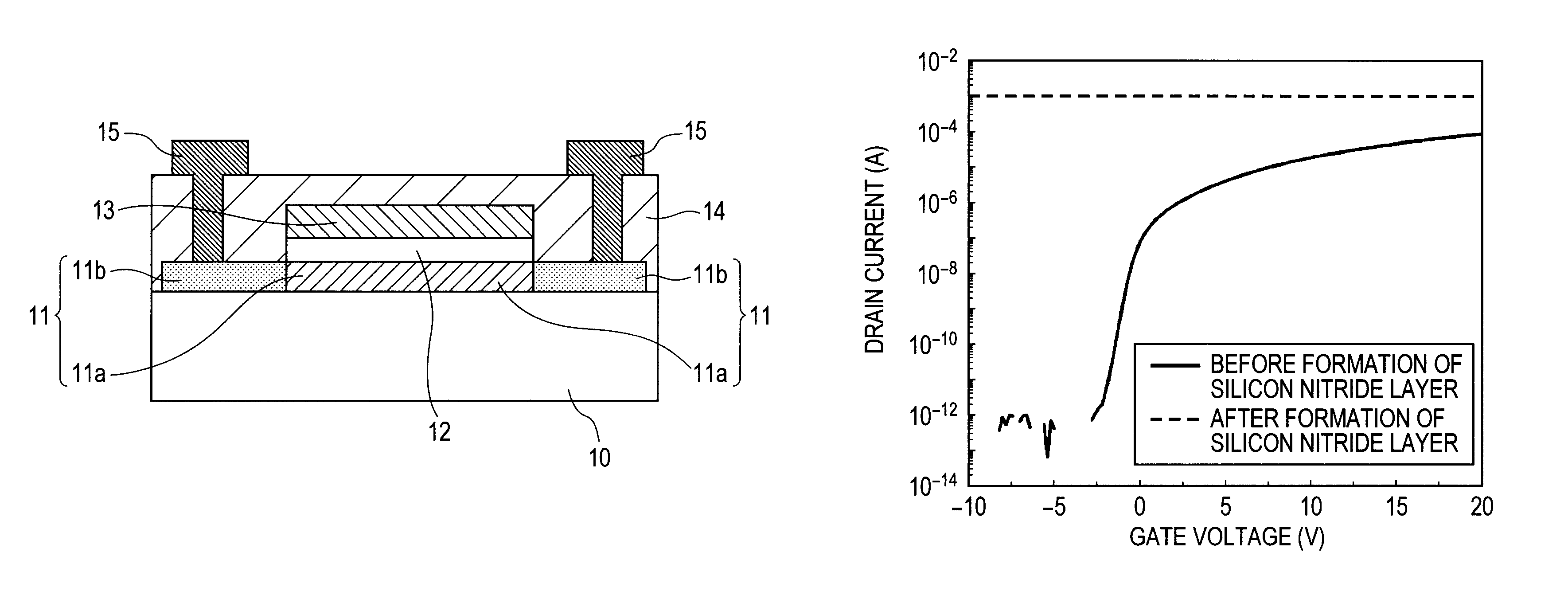
[0037]FIG. 1 illustrates an oxide semiconductor TFT having a top gate coplanar structure according to this example.

[0038]First, on the glass substrate 10, an amorphous IGZO film having a film thickness of 30 nm was formed as the oxide semiconductor layer 11 by a sputtering method. In order to form the oxide semiconductor layer 11, a DC sputtering apparatus was used and the substrate temperature was set to room temperature (25° C.). A target of a polycrystalline sintered body having an InGaZnO4 composition was used with the input DC power set to 300 W. During the film formation, the atmosphere was set to a total pressure of 0.5 Pa and the gas flow rate at that time was set to Ar:O2=98:2. After that, the oxide semiconductor layer 11 was patterned by a photolithography method and an etching method.

[0039]Next, on the oxide semiconductor layer 11 (on the channel region 11a of the oxide semiconductor layer), a silicon oxide film having a thickness of 100 nm was formed as the gate insulati...

example 2

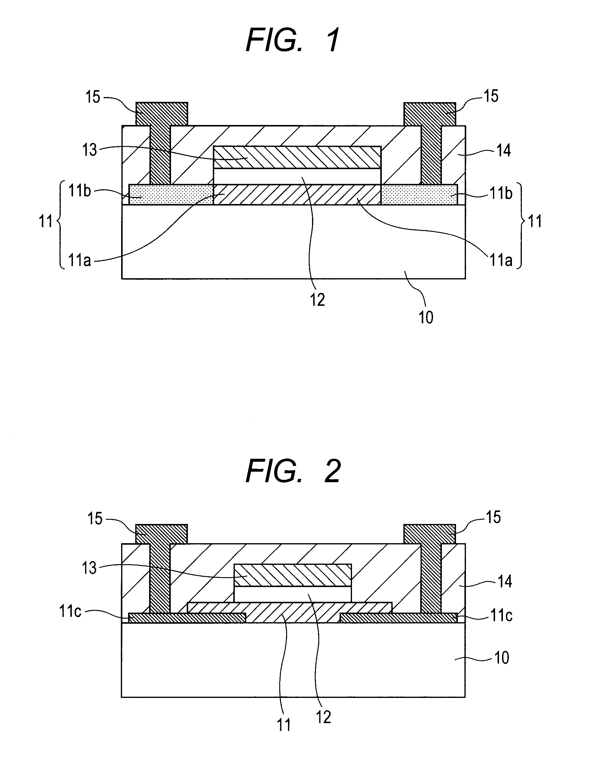
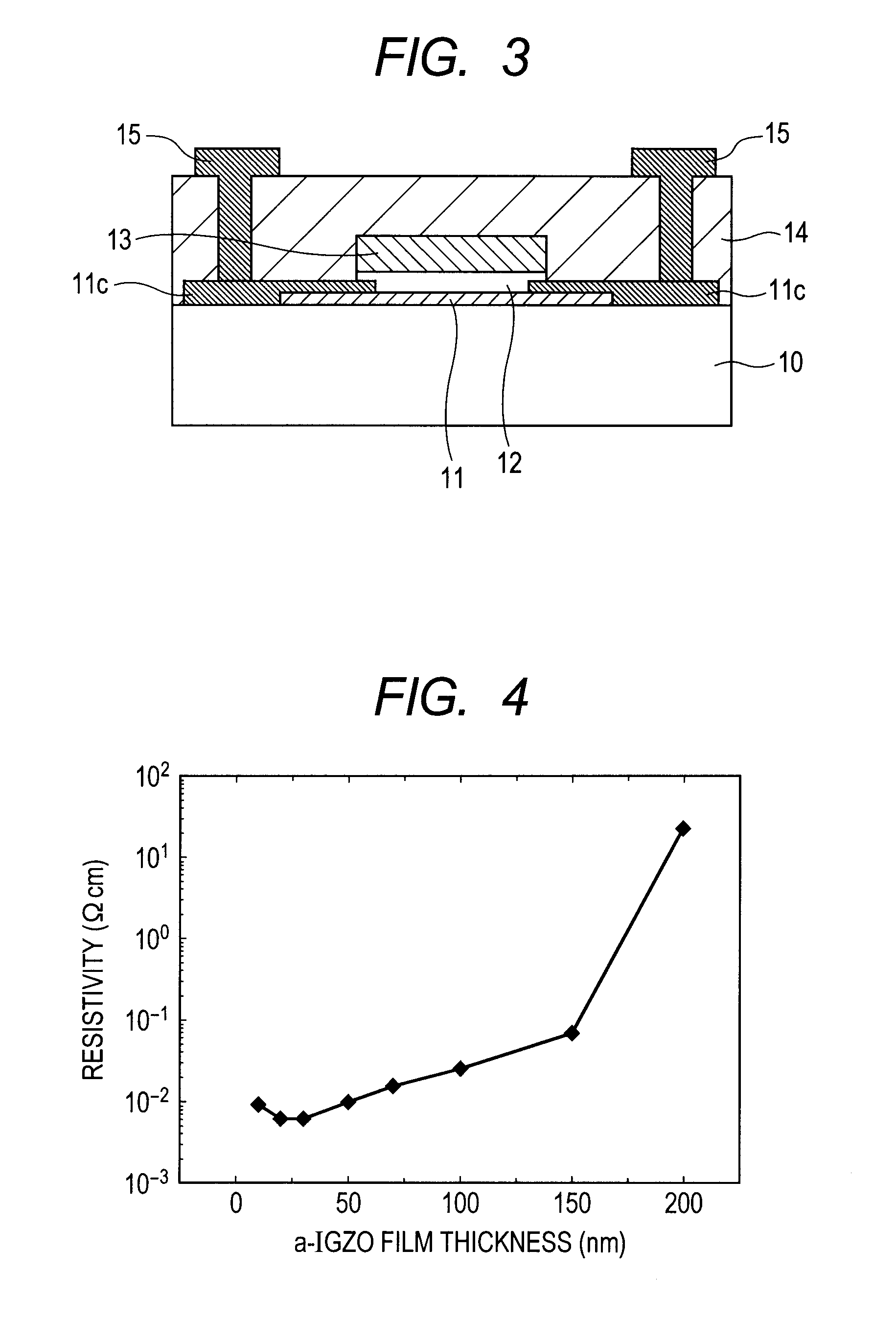
[0045]FIG. 2 illustrates an oxide semiconductor TFT having a top gate bottom contact structure according to this example.

[0046]First, on the glass substrate 10, an Mo film having a film thickness of 200 nm was formed as source and drain electrode layers 11c. After that, the source and drain electrode layers 11c were patterned by a photolithography method and an etching method.

[0047]Next, in the same manner as in Example 1, the oxide semiconductor layer 11 (channel region of the oxide semiconductor layer) and the gate insulating layer 12 were sequentially formed.

[0048]Subsequently, on the gate insulating layer 12, an amorphous IGZO film having a film thickness of 200 nm was formed as the gate electrode layer 13 by a sputtering method. The gate electrode layer 13 was formed at room temperature (25° C.) using a DC sputtering apparatus. A target of a polycrystalline sintered body having an InGaZnO4 composition was used with the input DC power set to 150 W. During the film formation, the...

example 3

[0053]FIG. 8 illustrates an oxide semiconductor TFT having a double gate coplanar structure according to this example.

[0054]First, on the glass substrate 10, an Mo film having a film thickness of 200 nm was formed as a bottom gate electrode layer 20. After that, the bottom gate electrode layer 20 was patterned by a photolithography method and an etching method.

[0055]Next, on the glass substrate 10 and on the bottom gate electrode layer 20, a silicon oxide film having a film thickness of 200 nm was formed as a lower gate insulating layer 21 by a plasma-enhanced CVD method. The substrate temperature was set to 340° C. in this plasma-enhanced CVD method for forming the silicon oxide film. SiH4 and N2O were used as a process gas. The gas flow rate was set to SiH4:N2O=1:25. The input RF power density and the pressure were set to 0.9 W / cm2 and 173 Pa, respectively.

[0056]Next, in the same manner as in Example 1, the oxide semiconductor layer 11 was formed.

[0057]Subsequently, on the oxide s...


PUM


Abstract

Provided is a top gate thin film transistor, including on a substrate: a source electrode layer; a drain electrode layer; an oxide semiconductor layer; a gate insulating layer; a gate electrode layer including an amorphous oxide semiconductor containing at least one kind of element selected from among In, Ga, Zn, and Sn; and a protective layer containing hydrogen, in which: the gate insulating layer is formed on a channel region of the oxide semiconductor layer; the gate electrode layer is formed on the gate insulating layer; and the protective layer is formed on the gate electrode layer.

Description

BACKGROUND OF THE INVENTION[0001]1. Field of the Invention[0002]The present invention relates to a top gate thin film transistor (top gate type thin film transistor) that uses an oxide semiconductor for a semiconductor layer, and a display apparatus including the top gate thin film transistor.[0003]2. Description of the Related Art[0004]Thin film transistors (TFTs) that use amorphous silicon or low-temperature polysilicon for a semiconductor layer are widely used in a drive circuit in display apparatuses such as active matrix liquid crystal display devices and organic electroluminescence (EL) display devices. However, the manufacture of those TFTs requires a high temperature process, and hence it is difficult to employ a flexible substrate such as a plastic substrate or a film substrate which is low in heat resistance.[0005]Meanwhile, in recent years, the development of TFTs that use, for a semiconductor layer, an oxide semiconductor having ZnO as a main component has recently becom...

Claims


Application Information

Patent Timeline
Patent Type & Authority Patents(United States)
IPC IPC(8): H01L29/786
CPCH01L29/78618H01L29/78648H01L29/66742H01L29/7869H01L29/66969
Inventor SATO, AYUMUKUMOMI, HIDEYAYABUTA, HISATOHAYASHI, RYOTAKAI, YASUYOSHI
Owner CANON KK
Why Eureka
Try Eureka