Strained semiconductor materials, devices and methods therefore

a technology of semiconductor materials and strain, applied in the field of semiconductor devices involving strained semiconductor materials, can solve the problems of low operating speed, high material cost, and limited wavelengths larger than about 1500 nm, and achieve the effect of reducing the relaxation of the strain

Inactive Publication Date: 2014-01-21
THE BOARD OF TRUSTEES OF THE LELAND STANFORD JUNIOR UNIV
View PDF14 Cites 7 Cited by
  • Summary
  • Abstract
  • Description
  • Claims
  • Application Information

AI Technical Summary

Benefits of technology

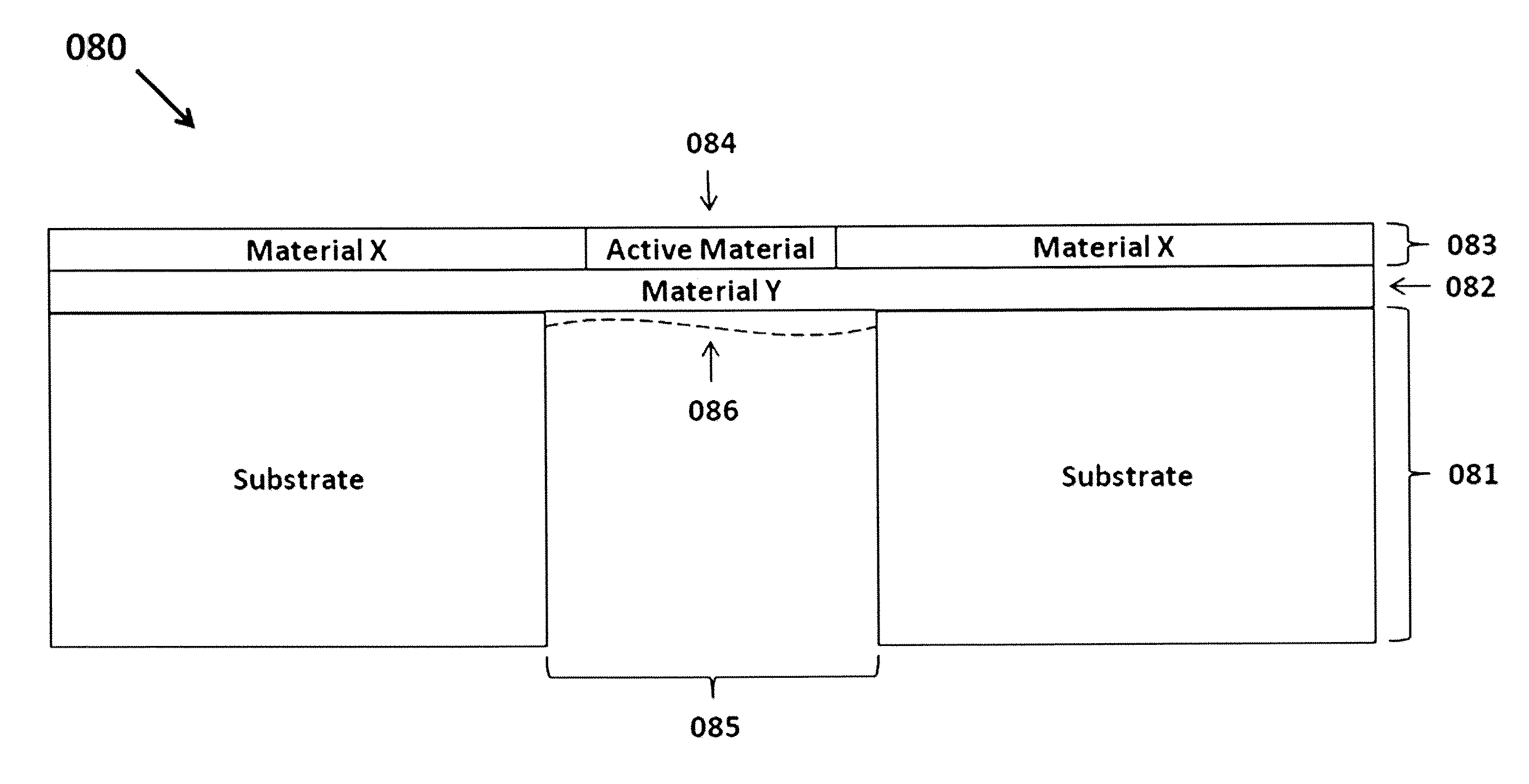
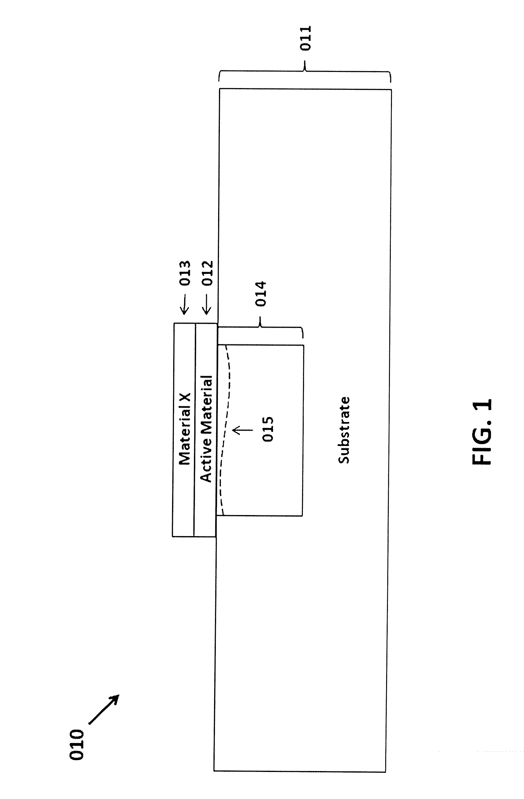
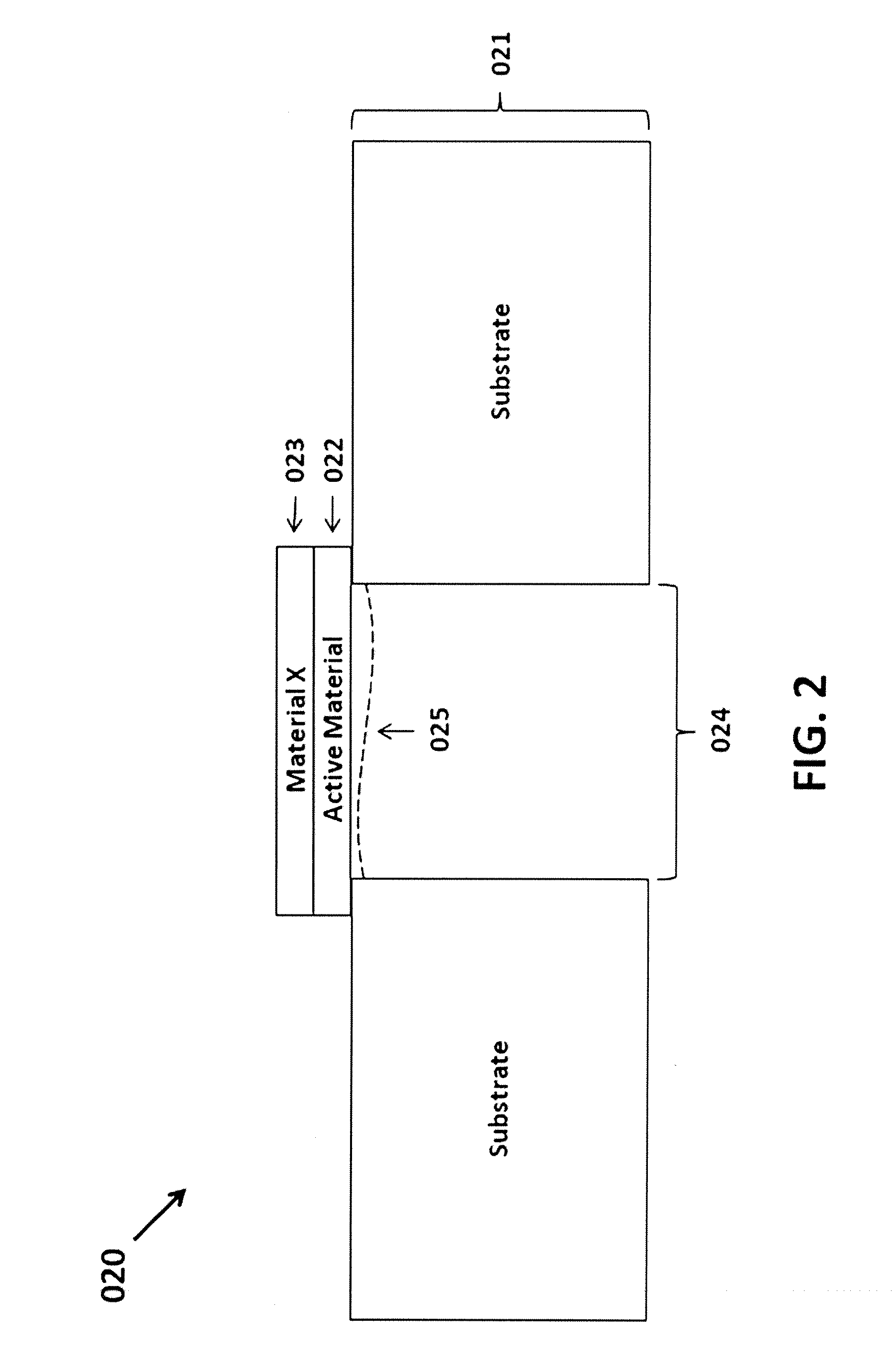
[0029]According to another example embodiment, a semiconductor device includes a substrate, a material stack, and a support structure to support the released material stack over a portion of the substrate. The material stack includes a first material over the substrate, an active material on the first material, and a second material on the active material. At least one of the first and second materials is configured and arranged to induce a strain in the active material, and at least one of the first and second materials is configured and arranged to mitigate relaxation of the strain induced in the active material.

Problems solved by technology

However, in light of a number of drawbacks concerning III-Vs, including process / fabrication complexity, high material costs, and incompatibility with silicon (Si), among others, some researchers have begun exploring alternatives to these traditional approaches to optoelectronics problems.
However, while bulk germanium may represent an attractive alternative to III-V materials for applications at the lower wavelength range, it suffers from limitations at wavelengths larger than about 1500 nm.
In particular, bulk germanium has an absorption coefficient at 1550 nm that is about 1 / 20th the absorption coefficients of some III-V materials (e.g. InGaAs), requiring a relatively thick germanium layer for comparable photodetection at this wavelength and resulting in low operating speeds.
In terms of light emission, germanium's optical output is especially weak due to several competing phenomena.
This less-than-optimal optoelectronic performance is directly related to the band structure of bulk germanium.
Unfortunately, germanium cannot efficiently absorb light energy at the band edges for several reasons.
In terms of light emission, the germanium band structure poses a more fundamental problem.
Thus, it is very difficult to make bulk germanium emit light without injecting an inordinately large amount of charge carriers.
Such high levels of carrier injection are impractical, requiring very high applied voltages and / or very low operating temperatures.
However, approaches to applying tensile strain to germanium in a silicon-compatible manner have fallen far short of the levels desired, involved material configurations that introduce drawbacks for final device performance and capabilities, and / or have involved complex fabrication processes that require particularly tight controls.
As a result of these complications and relative to telecommunications, for example, a large portion of the optical communications spectrum has been left relatively unsupported by germanium.
These and other matters have presented challenges to the design, manufacture and implementation of semiconductor devices, and in particular, of silicon-compatible devices such as those used in optoelectronics.

Method used


Image

  • Strained semiconductor materials, devices and methods therefore
  • Strained semiconductor materials, devices and methods therefore
  • Strained semiconductor materials, devices and methods therefore

Examples


example 2

Photodetectors

[0125]Following the general method of Example 1, a photodetector can be made on an active layer that is strained either prior to device fabrication or as the final step in the device fabrication process.

[0126]For example, a strained metal-semiconductor-metal (MSM) photodetector can be fabricated by adding a metal evaporation and photoresist lift-off lithography process after the method of Example 1 is followed to apply strain to an active layer meant to serve as the absorption medium in the device. In one specific process example, a spray-coating system can be used to deposit photoresist on all accessible material surfaces after the release etch is done for the strain transfer. Then, after photoresist exposure and developing to form electrode patterns, a metal electrode stack (e.g. 150 Å of Titanium followed by 350 Å of Gold) can be evaporated non-selectively on the wafer surface. A metal lift-off process consisting of soaking the wafer in a solvent (e.g. acetone) to d...

example 3

Light-Emitting Diodes

[0128]Following the general method of Example 1, a light-emitting diode (LED) can be made on an active layer that is strained either prior to device fabrication or as the final step in the device fabrication process. For example, a strained pin LED can be fabricated by combining the methods of Example 1 and Example 2 for the case of a pin photodetector.

[0129]As an alternate device example, a pn LED can be fabricated by combining the methods of Example 1 and Example 2 for the case of a pin photodetector but removing the intrinsic semiconductor from the material stack. In the case of epitaxially-obtained films, the starting active layer in this case could be comprised of two epitaxially-grown semiconductors, one of n-type doping and the other of p-type doping. Alternately, the starting active layer could be a single semiconductor of either n- or p-type doping. A subsequent ion implantation or other doping process can be done to introduce the opposite doping specie...

example 4

Photonic Crystals

[0130]Following the general method of Example 1, a photonic crystal can be made on an active layer that is strained either prior to device fabrication or as the final step in the device fabrication process.

[0131]For example, a strained photonic crystal can be fabricated by incorporating in the active layer pattern of Example 1 an additional pattern of holes of a desired size and arrangement to yield a photonic crystal in the active layer. In this approach, the hole pattern comprising the photonic crystal and the containing active layer pattern in which the holes are to be incorporated would be defined and etched simultaneously. Subsequent processing could proceed as normally described in the method of Example 1, with release etching done as normal or modified to also act through the photonic crystal holes in the active layer. The latter approach may be chosen to enhance the release etch rate, uniformity, mechanical integrity, and other factors of the active layer an...


PUM


Abstract

Various applications are directed to a material stack having a strained active material therein. In connection with an embodiment, an active material (e.g. a semiconductor material) is at least initially and partially released from and suspended over a substrate, strained, and held in place. The release and suspension facilitates the application of strain to the semiconductor material.

Description

CROSS-REFERENCE TO RELATED APPLICATION AND PRIORITY INFORMATION[0001]This application claims the benefit of U.S. Ser. No. 61 / 152,899 filed Feb. 16, 2009, which application is fully incorporated herein by reference.FIELD OF THE INVENTION[0002]The present invention relates generally to semiconductors, and more particularly to semiconductor devices involving strained semiconductor materials.BACKGROUND OF THE INVENTION[0003]A variety of electronic and optoelectronic fields and related devices use semiconductor materials to suit a variety of purposes. In many implementations, the properties of various materials used to make these devices are selected or otherwise tailored to suit specific applications.[0004]One of many representative semiconductor fields that have been of significant interest in recent times is the field of optoelectronics. The field of optoelectronics includes those materials, structures, devices, circuits, and systems that have properties appropriate for facilitating o...

Claims


Application Information

Patent Timeline
Patent Type & Authority Patents(United States)
IPC IPC(8): H01L29/06
CPCH01L33/34H01L31/105
Inventor JAIN, JINENDRA RAJAHOWE, ROGER T.
Owner THE BOARD OF TRUSTEES OF THE LELAND STANFORD JUNIOR UNIV
Why Eureka
Try Eureka